Semiconductor Wafer Analysis - A 2026 Perspective
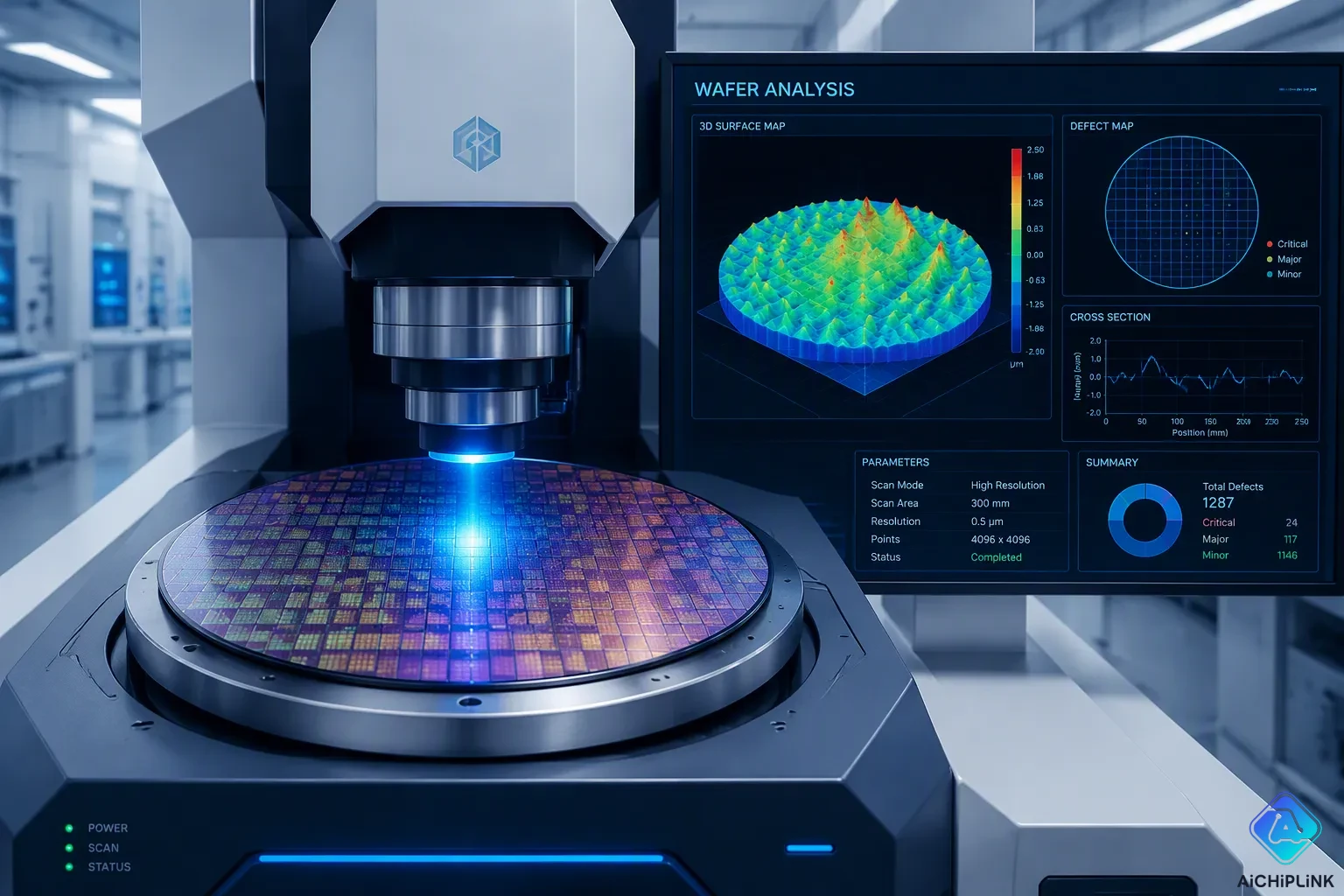
Semiconductor manufacturing now needs precision at atomic scales. Every defect, impurity, or size error can hurt yield and performance. Engineers use wafer analysis to catch these problems before they spread through production.
What does a full wafer analysis plan look like in 2026? This question pushes innovation across the industry. The field has changed a lot—from simple visual checks to advanced, data-driven methods.
Semiconductor wafers form the base for many uses, from smartphones to car electronics. The market pushes manufacturers to get higher yields while cutting costs. The market also wants faster time-to-market. Knowing the manufacturing process at every step has become key. Semiconductor production now depends on real-time data that links surface chemistry, electrical properties, and structural integrity of each wafer. These data help engineers make smart choices that protect profit and reliability across many uses.
Key Takeaways
-
Wafer analysis uses advanced tools like FTIR and SEM/EDS to spot defects early and improve chip yields.
-
Using several analysis methods together shows the full picture of wafer quality, which helps improve process control.
-
AI and statistical process control help predict and prevent yield loss, making production more efficient.
-
New trends like bigger wafers and advanced nodes need smarter, real-time monitoring to keep reliability high.
-
Engineers who use data-based wafer analysis stay ahead in the competitive semiconductor market.
Key Challenges in Wafer Testing
Surface Defects and Material Purity
Surface defects hurt yield in advanced chip making. Particles, scratches, and organic residues mess up device performance. The industry needs strict quality checks to catch these problems early. FTIR spectroscopy offers a dependable way to find organic contamination. This method looks for special C-H absorption peaks in the 3000–2800 cm⁻¹ range. A single-reflection 65-degree ATR tool with a Ge prism meets total reflection needs for high-refractive-index silicon samples. This setup gives a clean spectrum with a flat baseline. A case study using AFM-IR found organic contamination at thicknesses from 20 to 100 nm. The system matched a 30 nm residue to polyethylene terephthalate (PET) using a standard FTIR database. This proves FTIR works well for controlling wafer surface particle contamination.
Keeping material pure through the whole wafer making process stops yield loss. Contaminants can come from handling, storage, or process equipment. The market wants high-quality wafer materials for reliable uses in cars, consumer electronics, and industrial systems. Engineers must use wafer surface particle contamination control plans that include regular checks and cleaning. Proper wafer prep steps lower the chance of adding defects. These actions directly boost yield and device performance. The chip making environment needs strict rules to reduce contamination sources.
Dimensional Control and Reliability
Advanced nodes like 3nm bring extreme dimensional control challenges. Process variability and signal integrity issues need careful measurement. Old stuck-at fault models miss margin failures from interconnect coupling or substrate noise. Engineers must measure propagation delay across critical paths at 0.65V, 0–125°C, with supply noise of 50–100 mV in nanoseconds. ATE systems with real-time stimulus adjustment handle these needs. Power integrity poses another issue: current draw can exceed 500A in small areas on a 3nm 300mm wafer. Voltage sag risk requires checking that on-die voltage regulators respond correctly to load changes. Thermal management problems include local heat spikes over 100W/mm² from one test vector. Probe testing must support pitches ≤45µm while keeping signal integrity at multi-GHz speeds. Probe cards like FormFactor Altius allow verification at >3Gbps.
Reliability testing checks long-term performance under stress. Wafer-level reliability testing (WLRT) mimics working conditions like temperature extremes and voltage stress. Electromigration testing runs current through the wafer for a long time to measure resistance to metal movement. Environmental stress testing exposes wafers to extreme temperature, humidity, and other factors. These methods spot weaknesses early. The market for semiconductor devices in critical applications demands high reliability. Engineers must combine dimensional analysis with reliability testing to ensure performance. Chip production relies on data from these tests to boost yield and cut failures. Quality control protocols weave these findings into continuous improvement cycles.
Core Techniques for Silicon Wafers
Optical Inspection and SEM/EDS
Optical inspection is still the first way to find surface defects on silicon wafers. New systems now use artificial intelligence right in the imaging process. This makes defect detection faster and cuts down on false alarms that slow production. Engineers also use 3D and multi-pattern inspection tools to spot problems on complex wafer surfaces, which is key for advanced chip making. The industry is moving toward inline, real-time inspection that gives instant defect analysis, reducing downtime and improving process control. Sustainability also shapes equipment design, with energy-saving tools lowering costs and environmental impact.
For detailed defect analysis, scanning electron microscopy with energy-dispersive X-ray spectroscopy (SEM/EDS) gives elemental composition data. This combo identifies particle types and traces where they came from. Inline monitoring uses DR-SEM (defect review SEM) to classify defects automatically at production speed. This lets engineers tell killer defects from harmless particles without slowing down. The ability to analyze sub-micron features, defects, or particulate contaminants is very important for raising product yield in all industrial uses, including semiconductor device fabrication.
Surface and Electrical Analysis
Surface analysis methods show chemical states that optical tools cannot see. X-ray photoelectron spectroscopy (XPS) measures elemental composition and chemical bonding at the top few nanometers. Auger electron spectroscopy (AES) gives even better spatial resolution for nanoscale features. Fourier-transform infrared spectroscopy (FTIR) finds organic contamination through characteristic absorption bands. In one wafer fabrication failure analysis, field emission AES and small-area XPS jointly examined discolored bondpads. These failure analysis techniques performed surface composition analysis and depth profiling, identifying TiN residue as the root cause of nonstick bonding failure. The residue traced back to an under-etched ARC layer during bondpad opening. This analytical evidence directly guided the corrective action of increasing etch time.
Electrical testing completes the picture by measuring material quality directly. The four-point probe technique uses two probes to source current and two separate probes to measure voltage. This Kelvin configuration eliminates measurement errors from probe resistance, spreading resistance under each probe, and contact resistance between the metal probes and the semiconductor. Because the high-impedance voltmeter draws negligible current, the voltage drops across these parasitic resistances become very small, allowing accurate resistivity determination.
| Measurement | What it assesses | How it works |
|---|---|---|
| Four-probe | Resistivity / sheet resistance | Separates current-carrying contacts from voltage-sensing contacts; lead and contact resistances drop out; specific geometries convert measured resistance to resistivity via correction factors |
| Hall effect | Carrier density, carrier type, mobility | Adds perpendicular magnetic field to current; reads transverse voltage; sign of voltage gives carrier type; combined with resistivity yields mobility |
| Combined | Complete electrical characterization | Standard route from raw readings to publishable transport parameters |
These electrical measurements support quality control across the semiconductor wafers market. The market demands consistent wafer materials for diverse applications, from automotive power devices to consumer electronics. Proper wafer preparation ensures accurate readings. The market for analytical equipment continues expanding as applications multiply. Engineers combine dimensional analysis with electrical data to build complete wafer profiles. This integrated approach strengthens quality control and drives yield improvements across the industry.
The ability to analyze sub-micron features, defects, or particulate contaminants is of critical importance to increasing product yield in all industrial applications, including semiconductor device fabrication.
Data Integration for Wafer Insights
Multi-Technique Correlation
Each analytical method gives useful data on its own, but the real value shows up when engineers combine them. Multi-technique correlation links defect findings with electrical performance and chemical makeup. This turns separate measurements into useful knowledge for improving the process.
KLA Corporation's integrated failure analysis platform shows this approach in action. The platform pairs energy-dispersive X-ray spectroscopy (EDS) with X-ray photoelectron spectroscopy (XPS) to find contamination in semiconductors. The workflow follows a clear order: automated defect review uses EDS for fast elemental screening, then targeted XPS checks chemical bonding for key contamination sources. Machine learning algorithms match EDS elemental signatures with XPS chemical state data, which speeds up root cause identification.
These techniques work well together because each one has strengths the other lacks. EDS gives nanometer-scale spatial resolution for finding particles, while XPS offers surface sensitivity within 10nm depth. This pairing identifies where contamination comes from, such as cleaning residues, air exposure, or process chemical reactions. Labs use both methods in sequence: EDS first to locate contamination, then XPS for molecular identification and chemical bonding analysis of the found areas.
Cross-sectional preparation using focused ion beam milling enables subsurface contamination profiling, which adds to XPS surface analysis. Handling protocols must deal with contamination risks throughout the workflow, including glove use, clean-room environments, and dedicated storage containers. For comparative EDS-XPS studies, sample splitting or sequential analysis sequences must be set up, knowing that EDS under electron beam exposure may change surface chemistry that later XPS measurements can detect.
Correlation analysis goes beyond single defects to find yield-limiting factors across the whole manufacturing process. This statistical technique processes large volumes of manufacturing data to uncover hidden patterns and relationships that affect yield. Engineers correlate equipment data with manufacturing execution systems, track end-to-end wafer data from epitaxial processes to final test, and integrate feedback and feed-forward metrology data into process equipment. These correlations directly support quality control efforts and help engineers understand how surface defects impact final device performance across many applications.
AI and Statistical Process Control
Statistical process control (SPC) has long been the backbone of semiconductor quality management. Traditional SPC charts monitor process parameters and flag deviations from set baselines. Statistical Yield Limits within SPC help identify when a process stays statistically under control and when corrective actions become necessary. By telling apart normal and special variations, manufacturers improve quality and reliability, directly supporting yield prediction.
Modern AI-enhanced systems build on this foundation. Deep learning-based automatic defect classification improves accuracy for both existing and newly found defect types across various wafer designs. AI-based recipes generalize across multiple interconnect layers and integrated circuits in the back-end-of-line, increasing recipe creation and tuning efficiency. Vision foundation models use self-supervised learning on millions of unlabeled images to recognize new defect types with minimal retraining. In one study, PCB defect detection accuracy improved significantly using this approach.
Few-shot learning enables quick adaptation to new defect patterns or process changes. Vision language models generate interpretable natural language explanations and support interactive Q&A for engineers. These models also produce high-quality labels for downstream classification tasks, cutting model build times significantly compared to manual labeling.
Time series and lot-level analysis process both still images and video sequences to monitor process anomalies over time and prevent critical failures.
Predictive yield optimization turns yield from a lagging outcome into an earlier warning signal for process teams. Explainable yield-prediction frameworks combine diverse fabrication data with interpretable AI so teams can see which signals drive the forecast. Murphy's model calculates yield as a function of defect density and critical area, enabling estimation of the likelihood of producing defect-free semiconductor dies.
Long Short-Term Memory networks, autoencoders, and Random Forest classifiers identify subtle anomalies, capture multivariate correlations, and predict process deviations with significantly higher accuracy. These algorithms enhance yield prediction across the semiconductor market. The integration of AI with statistical process control strengthens wafer testing protocols and supports automated test equipment operations. Engineers who combine these tools gain deeper insights into process behavior, reduce costly excursions, and maintain competitive advantage in a demanding market. The semiconductor market continues expanding as new applications emerge, making robust data integration essential for manufacturers seeking operational excellence.
2026 Trends in Wafer Analysis
Larger Wafers and Advanced Nodes
The industry is moving to 300mm wafers for compound semiconductors like GaN and SiC. This change brings serious mechanical problems. Lattice mismatch between GaN and silicon, differences in thermal expansion, and wafer warpage during processing all threaten yield. As Infineon's Neyer explained, the stress is extremely high. The supply chain for 300mm Si(111) wafers is still not set up, which adds more complexity.
Advanced nodes at 3nm need atomic-level accuracy. Ultra-clean fabrication environments and advanced inspection systems must find tiny defects that make chips unusable. Process variation control, real-time monitoring, and AI-driven process correction become essential. Key metrics for evaluating wafer analysis equipment include defect density rates, CD uniformity, and first-pass yield performance. AI-enabled equipment supports real-time defect detection and adaptive process control, keeping yield consistent at these demanding nodes. Yield optimization drives requirements for predictive maintenance and machine learning-based process optimization across the manufacturing process.
In-Line Monitoring and Market Dynamics
In-line monitoring technologies now integrate directly into production lines. GBS's 3D surface measurement technology uses white light interferometry for high-resolution, non-contact analysis. These systems automatically incorporate into production lines, enabling continuous monitoring and documentation of product quality. X-ray and scatterometry techniques measure thin film thickness, density, and composition without destroying the wafer. Scatterometry tools analyze diffraction patterns to provide accurate measurements of critical dimensions and sidewall angles. These methods support thickness measurement, defect inspection, critical dimension measurement, and overlay metrology for semiconductor production.
Government-led reindustrialization shapes the silicon wafer market for 2026. The U.S. CHIPS Act, the European Chips Act, and India's Semicon India Program compel domestic wafer production and reduce import dependence.
Geopolitical factors also affect the market. US-China trade tensions create tariffs on silicon, contributing to price volatility. Regional conflicts and resource competition disrupt supply chains. Wafer reclamation emerges as a strategic buffer, enabling manufacturers to recycle existing wafers. Countries like China and South Korea invest heavily in domestic reclamation facilities to secure supply chains. These dynamics reshape procurement strategies across the silicon wafer market, driving demand for resilient sourcing and robust quality control in wafer fabrication.
Wafer analysis is changing fast to keep up with new chip designs, new materials, and bigger wafers. Engineers need to use many different tools and AI-powered insights to control quality well. This full approach turns raw data into clear choices that protect yield and reliability across many uses.
Making semiconductors requires constant change. The market rewards companies that use predictive analytics and real-time monitoring. Every wafer holds useful information about process health and device performance. The market for analysis tools grows as these needs increase. Engineers who check their current plans now set themselves up for success in 2026. The market rewards those who get ready for future challenges with strong, data-driven analysis systems.

Written by Jack Elliott from AIChipLink.
AIChipLink, one of the fastest-growing global independent electronic components distributors in the world, offers millions of products from thousands of manufacturers, and many of our in-stock parts is available to ship same day.
We mainly source and distribute integrated circuit (IC) products of brands such as Broadcom, Microchip, Texas Instruments, Infineon, NXP, Analog Devices, Qualcomm, Intel, etc., which are widely used in communication & network, telecom, industrial control, new energy and automotive electronics.
Empowered by AI, Linked to the Future. Get started on AIChipLink and submit your RFQ online today!
Frequently Asked Questions
How does FTIR detect organic contamination on wafers?
FTIR finds organic contamination on wafer surfaces by looking for unique absorption peaks. A single-reflection ATR tool with a Ge prism gives clear spectra. This method helps the wafer market. The market depends on this kind of analysis.
How does AI improve wafer defect classification?
AI systems use deep learning to sort wafer defects on their own. Vision models spot new defect types without much retraining. This tech cuts false alarms for high-performance uses. The semiconductor market rewards better yields. The market for AI tools keeps growing.
What challenges do larger wafers for compound semiconductors create?
Switching to larger wafers for GaN and SiC causes stress problems for these compound semiconductors. Lattice mismatch hurts yield. These compound semiconductors need special handling. The market wants answers for wafer issues. The global market adjusts to new materials.
Why do engineers combine EDS and XPS for wafer analysis?
Engineers pair EDS with XPS for chemical analysis across wafer samples. This connection finds contamination sources. The approach helps the silicon wafer market. The market gains from these methods.
What drives the wafer analysis equipment market in 2026?
The market for analytical equipment grows as advanced nodes need precision on every wafer. In-line monitoring becomes vital for wafer analysis. The silicon wafer market grows with new uses. Many uses need steady quality. The competitive market pushes innovation.