The ATMEGA328P-AU is a popular microcontroller from Microchip Technology, widely used in various embedded systems due to its robust performance, versatility, and ease of use. It belongs to the AVR family of microcontrollers and is known for its low power consumption, making it an ideal choice for battery-powered applications. This article delves into the essential aspects of the ATMEGA328P-AU, covering its datasheet, pinout, schematic, footprint, programming, and other relevant features.
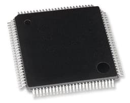
Product shown in the picture: ATMEGA328P-AU
ATMEGA328P-AU Datasheet Overview
The ATMEGA328P-AU datasheet is the first resource you should consult to understand the microcontroller's specifications and features. This document provides detailed information about the microcontroller's architecture, electrical characteristics, memory, and peripherals. Key specifications include:
Operating Voltage: 1.8V - 5.5V
Flash Memory: 32KB
SRAM: 2KB
EEPROM: 1KB
Clock Speed: Up to 20 MHz
GPIO Pins: 23 (with individual programmable pull-up resistors)
The datasheet also includes information about the microcontroller’s power consumption in various modes, such as active, idle, and sleep modes. Understanding these details is crucial for optimizing your design for low power applications.
ATMEGA328P-AU Pinout Configuration
The ATMEGA328P-AU pinout is a critical aspect when designing your circuit. The microcontroller comes in a 32-pin TQFP (Thin Quad Flat Package) or VQFN (Very Thin Quad Flat No-lead) package, making it compact and suitable for space-constrained applications.
Here’s a brief overview of the ATMEGA328P-AU pinout:
• VCC/GND: These pins provide power and ground connections to the microcontroller.
Port B (PB0-PB7): These are 8-bit bi-directional I/O pins with internal pull-up resistors. They also serve as inputs to the Analog-to-Digital Converter (ADC).
• Port C (PC0-PC6): These pins can function as either digital I/O or analog inputs.
• Port D (PD0-PD7): Similar to Port B, these are digital I/O pins that can also serve various peripheral functions.
• RESET: This pin is used to reset the microcontroller.
• XTAL1/XTAL2: These pins are used for connecting an external crystal oscillator, which provides the clock source for the microcontroller.
• AVCC: This pin supplies power to the ADC. It should be connected to VCC through a low-pass filter to improve ADC performance.
• AREF: This pin provides the reference voltage for the ADC.
ATMEGA328P-AU Schematic Design Considerations
When designing a schematic with the ATMEGA328P-AU, several considerations must be taken into account to ensure proper functionality. The power supply design is crucial, as the microcontroller operates at different voltages depending on the application. A decoupling capacitor of 0.1µF should be placed as close as possible to the VCC and GND pins to reduce noise.
For the crystal oscillator, a pair of capacitors (typically 22pF) should be connected to the XTAL1 and XTAL2 pins. These capacitors stabilize the oscillator and ensure accurate clock generation. Additionally, if your application requires an external reset button, connect it to the RESET pin with a pull-up resistor (typically 10kΩ) to VCC.
The schematic should also include connections for In-System Programming (ISP), which is essential for uploading code to the microcontroller. Typically, an ISP header with connections to MOSI, MISO, SCK, RESET, VCC, and GND is included.
ATMEGA328P-AU Footprint and PCB Layout
The ATMEGA328P-AU footprint refers to the physical layout of the pins on the printed circuit board (PCB). For the TQFP package, the footprint includes 32 pads arranged in a 7mm x 7mm square with a 0.8mm pitch between pins. Proper alignment of the footprint with the package is crucial to ensure reliable soldering and electrical connections.
When designing the PCB layout, special attention should be given to the routing of the power and ground traces to minimize noise and ensure stable operation. The AVCC pin should be connected to VCC through a low-pass filter, and the AREF pin should be connected to the desired reference voltage, typically with a decoupling capacitor to ground.
The PCB layout should also account for the placement of bypass capacitors near the power pins and provide sufficient trace width for high-current paths. For analog circuits, keep analog and digital grounds separate to reduce noise interference.
ATMEGA328P-AU Programming and Development
Programming the ATMEGA328P-AU is straightforward, thanks to its compatibility with the popular Arduino platform. The Arduino IDE provides a user-friendly environment for writing, compiling, and uploading code to the microcontroller. The ATMEGA328P-AU can be programmed using various methods, including:
• In-System Programming (ISP): This method uses a programmer, such as the AVRISP mkII, to upload code directly to the microcontroller via the ISP header.
• Bootloader: The ATMEGA328P-AU can be programmed using a bootloader, which allows for code upload via a serial interface (UART) without the need for an external programmer.
• JTAG: For advanced debugging and programming, the JTAG interface can be used, although this requires additional hardware and software support.
Applications and Use Cases
The ATMEGA328P-AU is widely used in various applications due to its versatility and low power consumption. Common use cases include:
• Arduino Boards: The ATMEGA328P-AU is the heart of many Arduino boards, including the popular Arduino Uno. It provides the processing power for a wide range of DIY and professional projects.
• IoT Devices: Thanks to its low power consumption, the ATMEGA328P-AU is ideal for Internet of Things (IoT) devices that require long battery life.
• Consumer Electronics: The microcontroller is used in various consumer electronics, from remote controls to smart home devices.
Industrial Automation: In industrial settings, the ATMEGA328P-AU is employed in control systems, sensors, and other automation equipment.
Conclusion
The ATMEGA328P-AU is a versatile and powerful microcontroller that offers a wide range of features suitable for various applications. Understanding its datasheet, pinout, schematic design considerations, footprint, and programming methods is essential for maximizing its potential in your projects. Whether you are designing a simple embedded system or a complex IoT device, the ATMEGA328P-AU provides a reliable and efficient solution.