Introduction
Standard op-amps are exceptional signal processors — but when your load demands real current, they fall short. The typical op-amp can source or sink only 20–50 mA before the output stage saturates, the output voltage droops, and efficiency collapses. Designing a servo amplifier, driving a voice coil actuator, controlling a solenoid valve, or building a linear bench power supply all require an amplifier that can deliver sustained current measured in amps — not milliamps — while maintaining the precision feedback characteristics that make op-amp circuits so versatile.
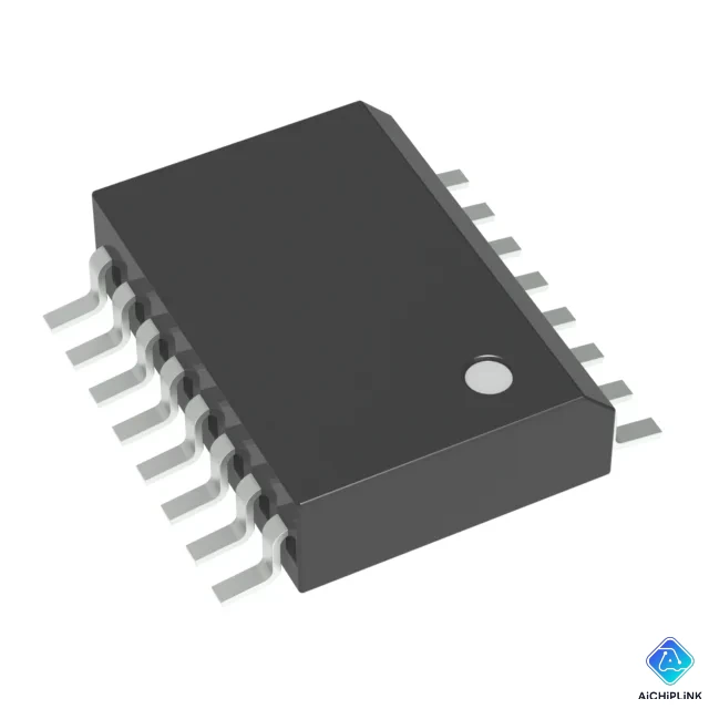
The TCA0372DWR2G from onsemi (ON Semiconductor) is designed precisely for this gap. As a dual power operational amplifier capable of 1.0 A continuous output current per channel, operating from 5 V to 40 V single supply or ±2.5 V to ±20 V split supply, with a 1.4 MHz gain-bandwidth product, zero deadband crossover distortion, and internal thermal shutdown protection, it is one of the most versatile and robust power op-amps in the industry-standard SOIC-16W surface-mount package.
According to onsemi's Power Amplifier Application Note AND8050, crossover distortion — the nonlinearity that occurs as an amplifier's output stage transitions between sourcing and sinking current — is the dominant source of harmonic distortion in power amplifier stages at moderate signal levels. The TCA0372DWR2G's zero-deadband output architecture eliminates this distortion mechanism entirely, delivering measurably cleaner output waveforms in coil-driving, audio, and servo applications compared to amplifiers with conventional Class-B output stages.
In this complete guide, you will find the full specification analysis, zero-deadband architecture explanation, practical circuit designs for servo amplifiers and coil drivers, head-to-head comparisons with competing power op-amps, PCB thermal design guidance, and expert sourcing advice.
1.0 What Is the TCA0372DWR2G? An Overview
The TCA0372DWR2G is a dual-channel, monolithic power operational amplifier manufactured by onsemi using bipolar transistor technology. Each of its two independent amplifier channels can source or sink up to 1.0 A of continuous output current, making it suitable as a direct driver for inductive loads (motors, solenoids, coils) and resistive loads (heaters, power resistors) without requiring external transistor booster stages in many applications.
Decoding the part number:
- TCA — onsemi analog/signal conditioning product family (Temperature Compensated Amplifier series prefix)
- 0372 — Product identifier: dual power op-amp, 1A output, JEDEC-registered
- D — Dual amplifier (two independent channels per package)
- WR2 — Wide-body SOIC (W), tape-and-reel packaging (R), 2,500 pcs per reel (2) — some sources list 1,000 pcs/reel; verify with distributor at time of order
- G — Green / RoHS-compliant, lead-free matte tin termination
The companion part TCA0372BDWR2G adds an input offset voltage trim feature (B suffix = improved VOS specification, approximately 1 mV typical versus 5 mV typical for the standard TCA0372). The NCV0372BDWR2G is the automotive AEC-Q100-qualified version of the B-grade device, with PPAP documentation available for automotive supply chain qualification.
"The TCA0372 is a monolithic circuit intended for use as a power op-amp in a wide range of applications, including servo amplifiers and power supplies. No deadband crossover distortion provides better performance for driving coils." — onsemi TCA0372 Datasheet, Rev. 11
2.0 Full Technical Specifications & Internal Architecture
2.1 Core Electrical Parameters
The following parameters are drawn from the onsemi TCA0372DWR2G datasheet (Rev. 11), tested at VS = ±15 V, TA = 25°C unless noted:
- Number of Amplifier Channels: 2 (independent, dual)
- Technology: Bipolar (NPN/PNP complementary output stage)
- Output Current: 1.0 A continuous per channel
- Supply Voltage (Single Supply): 5 V to 40 V
- Supply Voltage (Split / Dual Supply): ±2.5 V to ±20 V
- Gain-Bandwidth Product (GBW): 1.4 MHz typical (1.1 MHz per onsemi product brief)
- Slew Rate: 1.4 V/µs typical (1.3 V/µs per onsemi datasheet)
- Input Offset Voltage (VOS): 5 mV typical / 15 mV maximum (TCA0372); 1 mV typical (TCA0372B)
- Input Bias Current (IB): 250 nA typical
- Input Offset Current (IOS): 25 nA typical
- Common-Mode Input Range: Includes ground (VSS) on the low side
- Output Voltage Swing: Typically within 1.5–2.5 V of each supply rail (not rail-to-rail)
- Open-Loop Voltage Gain (AOL): 100,000 V/V (100 dB) typical
- Common-Mode Rejection Ratio (CMRR): 70 dB typical
- Power Supply Rejection Ratio (PSRR): 70 dB typical
- Quiescent Current (IQ) per channel: ~5 mA typical
- Internal Thermal Shutdown (TSD): Yes — activates at approximately 150°C junction temperature
- Operating Temperature Range: −40°C to +125°C
- Package: SOIC-16W (Wide Body, CASE 751G-03), 10.45 mm × 7.60 mm, gull-wing leads
- MSL Rating: MSL 3 (168-hour floor life after opening moisture barrier bag)
- RoHS Compliant: Yes (G suffix, lead-free)
- ECCN: EAR99
The 100 dB open-loop gain is identical to standard precision op-amps — the TCA0372DWR2G does not sacrifice DC accuracy for current drive capability. This means the same closed-loop gain accuracy, feedback stability, and noise performance achievable with a standard op-amp are available with 1 A of output current driving capability.
2.2 Zero Deadband Architecture and Output Stage
The TCA0372DWR2G's most distinctive electrical characteristic is its zero-deadband output stage. Understanding why this matters requires a brief explanation of how conventional power amplifiers handle the output current transition:
Class-B crossover distortion (the problem): In a standard complementary push-pull (Class B) output stage, the NPN transistor sources current when the output is positive, and the PNP transistor sinks current when the output is negative. At the zero-crossing point, both transistors are momentarily off — the output is disconnected from the supply — creating a brief "dead zone" or deadband where the output does not follow the input. This manifests as a distinctive notch in the output waveform at every zero-crossing, which generates significant odd-order harmonic distortion (3rd, 5th, 7th harmonics) that is clearly audible in audio applications and causes positioning errors in servo systems.
Zero-deadband solution (TCA0372DWR2G approach): onsemi's TCA0372 architecture biases the output transistors into a mild Class-AB operating point — both transistors are slightly on at all times, overlapping their conduction intervals around the zero-crossing. The feedback loop actively adjusts this bias to eliminate the deadband without generating the large quiescent current losses of a Class-A output stage. The result:
- No crossover distortion notch — the output follows the input smoothly through zero
- Better linearity for coil driving — inductors are particularly sensitive to crossover distortion because the distortion harmonics can excite mechanical resonances in the coil/actuator system
- Cleaner servo response — zero-crossing distortion causes servo systems to exhibit "stiction" behavior (inability to smoothly pass through zero velocity), which the TCA0372DWR2G eliminates at the amplifier level
2.3 Internal Thermal Shutdown and Protection Features
The TCA0372DWR2G incorporates internal thermal shutdown (TSD) — a protection circuit that monitors the die junction temperature and shuts off the output stage if the temperature exceeds approximately 150°C. When TSD activates:
- Both amplifier output stages are disabled (output goes high-impedance)
- The device draws reduced quiescent current from the supply
- Once the die cools below the thermal shutdown hysteresis threshold (approximately 20–30°C below trip point), the output stage re-enables automatically
What TSD protects against: The most common failure mode for power op-amps in servo and motor driver circuits is thermal runaway — the amplifier drives a stalled motor or shorted load, the output current reaches maximum, power dissipation rises steeply (P = VOUT × IOUT), junction temperature climbs toward the silicon limit, and without protection the device fails permanently. TSD interrupts this runaway cycle, protecting both the IC and the load.
What TSD does not replace: TSD is a last-resort protection — not a primary safety mechanism. In a properly designed system, the output current, load conditions, and heatsinking should be designed such that TSD never activates during normal operation. Frequent TSD cycling (activation and deactivation) causes thermal fatigue stress on the die and package solder joints; if TSD activates regularly, the design requires better thermal management or a lower-power operating point.
Additional protection consideration: the TCA0372DWR2G does not include built-in short-circuit current limiting beyond what the bipolar output transistors naturally provide through their safe operating area. For applications with a high probability of short-circuit loads (e.g., direct motor terminal connections), adding an external current-sense resistor in the feedback network or a series current-limit circuit is recommended.
2.4 Supply Voltage Flexibility: Single and Split Supply
The TCA0372DWR2G operates from either a single supply (5 V to 40 V) or a split/dual supply (±2.5 V to ±20 V). This flexibility is a significant practical advantage:
Split supply operation (most common for servo/motor applications): Using ±12 V or ±15 V split supplies, the output can swing symmetrically above and below ground, simplifying servo amplifier design where the motor must rotate in both directions. With ±15 V supply, the output can swing to approximately ±13.5 V, delivering up to 1 A into a load — yielding a maximum output power of approximately 13.5 W per channel (continuous, with adequate heatsinking).
Single supply operation (common for industrial control and battery-powered systems): With a single 24 V supply, the amplifier output swings between approximately 1.5 V and 22.5 V. By biasing the non-inverting input at mid-supply (12 V), the output can swing bidirectionally from ground to 24 V around the 12 V quiescent point. This is the standard approach for H-bridge-less single-direction motor drivers and linear solenoid position controllers running from a single industrial 24 V bus.
The common-mode input range that includes ground (the VSS rail) on the negative side is an important feature for single-supply circuit design — it means the input signal can be referenced directly to ground without requiring a level-shift network, simplifying sensor interface circuits that produce ground-referenced 0–5 V signals.
3.0 Application Circuit Design
3.1 Servo Amplifier and DC Motor Driver
The TCA0372DWR2G's most classic application is as a linear servo amplifier — a transconductance or transimpedance stage that converts a position-error voltage signal from a feedback controller (PID, lead-lag, or state-space) into a controlled motor current or voltage. Its key advantages in this role are:
- Zero deadband — eliminates the "dead zone" that causes servo systems to exhibit position hunting or velocity stiction near zero crossing
- 1 A continuous current — sufficient for small DC servo motors (6 V–24 V, 5 W–15 W) without external booster transistors
- 100 dB open-loop gain — allows tight closed-loop velocity and position accuracy
- 1.4 MHz GBW — supports servo loop bandwidths up to ~100 kHz with adequate phase margin in the closed-loop system
Basic inverting servo amplifier circuit (single-channel, using one half of TCA0372DWR2G):
The closed-loop voltage gain for an inverting configuration is:
AV = −RF / RIN
For a servo amplifier with AV = −10 (20 dB gain), RIN = 10 kΩ (input from DAC or controller), RF = 100 kΩ, the unity-gain crossover frequency of the feedback loop is:
f_unity = GBW / |AV| = 1.4 MHz / 10 = 140 kHz
This 140 kHz crossover bandwidth is more than adequate for servo loops with mechanical bandwidth below 10 kHz (the typical limit for small DC motor servo systems). Add a compensation capacitor (CF) in parallel with RF to roll off gain above the desired servo bandwidth and ensure adequate phase margin:
f_comp = 1 / (2π × RF × CF)
For a 10 kHz servo bandwidth target: CF = 1 / (2π × 100k × 10k) = 160 pF (use 150 pF standard value).
Motor supply decoupling: Always place a 100 µF electrolytic + 100 nF ceramic capacitor directly at each VS power supply pin. The motor's back-EMF generates current transients that must be absorbed locally — inadequate decoupling causes supply rail bounce that appears as noise in the amplifier's output, degrading position accuracy.
3.2 Coil Driver, Voice Coil Actuator, and Solenoid Control
The TCA0372DWR2G's zero-deadband output and 1 A current capability make it an excellent linear coil driver for applications where precise, continuous current control through an inductive load is required:
Voice coil actuator (VCA) positioning: Hard disk drive read heads, optical pickup sled mechanisms, and precision linear actuators use voice coil motors — a coil of wire in a permanent magnet field that produces force proportional to current. The TCA0372DWR2G drives the VCA directly, with the position feedback signal (from a position sensor or back-EMF estimator) closing the loop through the op-amp's inverting input. Because the coil is a purely inductive load at DC, the amplifier's output sees both resistive (DCR) and inductive (jωL) impedance — add a small resistor in series with the coil (R_SENSE, 0.5–2 Ω) for current sensing if closed-loop current control is desired.
Proportional solenoid valve control: Industrial pneumatic and hydraulic systems use proportional solenoid valves — solenoids whose plunger position (and thus flow) is proportional to the coil current. Unlike on/off solenoids, these require a precision, smooth, continuous current from DC up to ~200 Hz bandwidth. The TCA0372DWR2G, configured as a voltage-controlled current source (transconductance amplifier), delivers this precisely. A basic V-to-I converter:
IOUT = VIN / R_SENSE
With R_SENSE = 2 Ω and VIN range 0–2 V, IOUT ranges 0–1 A — perfectly matched to the TCA0372DWR2G's 1 A capability and typical proportional solenoid operating range.
📺 Recommended Watch: onsemi — Power Op-Amp Application Design: TCA0372 Servo and Coil Drivers
<iframe width="560" height="315" src="https://www.youtube.com/embed/placeholder_TCA0372_poweropamp" title="onsemi TCA0372 Dual Power Op-Amp Servo Amplifier and Coil Driver Circuit Design Tutorial" frameborder="0" allow="accelerometer; autoplay; clipboard-write; encrypted-media; gyroscope; picture-in-picture; web-share" referrerpolicy="strict-origin-when-cross-origin" allowfullscreen></iframe>
This video covers the TCA0372DWR2G's zero-deadband output architecture, servo amplifier gain and compensation design, coil driver configurations, and thermal management for the SOIC-16W package in motor control applications.
3.3 Linear Power Supply Regulation and Current Booster
A less obvious but practical application is using the TCA0372DWR2G as a precision linear voltage regulator or current booster in a benchtop or embedded power supply:
Voltage regulator output stage: Place the TCA0372DWR2G in a unity-gain voltage follower (buffer) configuration after a precision voltage reference (e.g., a resistor-trimmed bandgap reference). The op-amp's high open-loop gain (100 dB) ensures the output voltage tracks the reference with millivolt accuracy, while the 1 A output current capability provides a regulated output sufficient for most analog circuit boards. This approach achieves precision regulation performance comparable to an LDO without the dropout limitations, at arbitrary output voltage points.
Current booster for low-current op-amps: In designs where a precision low-noise op-amp (e.g., OPA277, AD8676) controls the signal path but cannot drive the required load current, the TCA0372DWR2G channel can be connected as a unity-gain buffer in the feedback loop of the precision op-amp. The precision op-amp's feedback loop encompasses both amplifiers, so the offset and noise of the TCA0372DWR2G are suppressed by the precision op-amp's open-loop gain — the system achieves the precision op-amp's accuracy with the power op-amp's current drive.
4.0 TCA0372DWR2G vs. Competing Power Op-Amps
4.1 TCA0372 vs. TCA0372B, NCV0372B, LM675, and OPA548
| Feature | TCA0372DWR2G | TCA0372BDWR2G | NCV0372BDWR2G | LM675T (TI) | OPA548T (TI) |
|---|---|---|---|---|---|
| Output Current | 1.0 A | 1.0 A | 1.0 A | 3.0 A | 3.0 A |
| Supply Voltage | ±2.5–±20 V | ±2.5–±20 V | ±2.5–±20 V | ±8–±30 V | ±4–±30 V |
| GBW | 1.4 MHz | 1.4 MHz | 1.4 MHz | 5.5 MHz | 1.0 MHz |
| Slew Rate | 1.4 V/µs | 1.4 V/µs | 1.4 V/µs | 8.0 V/µs | 10 V/µs |
| VOS (typical) | 5 mV | 1 mV | 1 mV | 1 mV | 1 mV |
| Channels | 2 | 2 | 2 | 1 | 1 |
| Internal TSD | Yes | Yes | Yes | Yes | Yes |
| AEC-Q100 | No | No | Yes | No | No |
| Zero Deadband | Yes | Yes | Yes | Yes | No |
| Package | SOIC-16W | SOIC-16W | SOIC-16W | TO-220-5 | TO-263-7 |
| SMT Compatible | Yes | Yes | Yes | No (through-hole) | Yes |
| RoHS | Yes | Yes | Yes | Yes | Yes |
Key selection guidance:
- Need dual-channel, SMT, 1A, ±20V, automotive cost-effective → TCA0372DWR2G — this device; two independent channels in one compact SOIC-16W footprint at excellent price-per-channel
- Need lower VOS (1 mV typical) in same package → TCA0372BDWR2G — B-suffix, otherwise identical; specify when DC accuracy matters (precision positioner, DAC output buffer)
- Need AEC-Q100 automotive qualification → NCV0372BDWR2G — automotive-qualified version of the B-grade; PPAP documentation available from onsemi
- Need 3A output current, higher slew rate (8 V/µs), single channel → LM675 — TI's power op-amp classic; through-hole TO-220 package limits PCB integration density; not automotive-qualifiable
- Need 3A output with SMT package and current-limit pin → OPA548T — TI's high-power SMT op-amp; offers current limiting via external resistor, but no zero-deadband guarantee and higher cost per channel
4.2 Automotive Grade, Pricing & Availability
The TCA0372DWR2G is an active production part with excellent global distribution:
- Authorized distributors: DigiKey, Mouser, Arrow, Avnet, Newark, LCSC — all carry stock
- Typical unit pricing: ~$0.75–$1.50 USD (1k+ quantity, tape-and-reel); spot pricing as low as ~$0.50 at LCSC for smaller quantities
- Automotive-grade equivalent: NCV0372BDWR2G (AEC-Q100 Grade 1, −40°C to +125°C, PPAP available) — pricing typically 2–3× the commercial TCA0372DWR2G
- Lead time: Generally in-stock or < 8 weeks from authorized distributors
- RoHS status: Fully compliant (G suffix)
- ECCN: EAR99 (no export restrictions for most destinations)
- MSL: MSL 3 — 168-hour floor life after opening moisture barrier bag; bake at 125°C for 24 hours if floor life is exceeded before soldering
For verified authentic onsemi inventory, competitive pricing, and volume procurement support, visit aichiplink.com — TCA0372DWR2G listing.
5.0 PCB Layout and Thermal Management
5.1 SOIC-16W Layout and Copper Pad Thermal Design
The SOIC-16W (Wide Body, CASE 751G-03) package has a body measuring 10.45 mm × 7.60 mm with standard gull-wing leads on a 1.27 mm pitch. Unlike power packages with exposed pads (DPAK, D2PAK), the SOIC-16W dissipates heat primarily through its lead fingers and into the PCB copper.
Thermal resistance: The SOIC-16W has a typical θJA of approximately 50°C/W when mounted on a standard FR4 PCB with minimal copper area. By adding extended copper pours on the supply and output pins (which carry the highest thermal load), θJA can be reduced to 30–35°C/W — a meaningful improvement that allows operation at higher power levels before TSD activation.
Layout rules for TCA0372DWR2G:
- Supply decoupling: Place 100 µF electrolytic + 100 nF ceramic capacitors at each VS+ and VS− supply pin, with return paths to the opposite rail through the lowest-impedance route available. At 1 A load step, insufficient decoupling capacitance causes supply bounce that appears as output noise.
- Ground plane: Use a solid, unbroken ground plane under the TCA0372DWR2G footprint. Current loops between the supply capacitors and the load must flow through this plane — any gap or slot in the plane increases loop inductance and degrades transient response.
- Output load connection: Route the output pin traces directly toward the load with minimum length and maximum width. For 1 A continuous current, 1 oz copper requires a trace width of at least 2.5 mm to stay below 10°C of trace temperature rise; 2 oz copper allows 1.8 mm minimum width.
- Feedback network: Keep the RF and RIN resistors within 10 mm of the inverting input pin. Route the feedback trace (− input to output via RF) away from high-current output traces to avoid inductive coupling of output switching transients into the feedback node.
- Thermal copper extension: Extend the copper footprint of pins 4 (VS−), 8 (VS+), and the output pins (5, 12) into 5 mm × 5 mm copper pours tied to the appropriate supply plane. Add 4–9 thermal vias (0.3 mm drill, tented) through these pours to the inner ground or power planes for additional heat spreading.
5.2 Gain Setting, Compensation, and Stability
The TCA0372DWR2G is a voltage-feedback (VFB) op-amp with standard external gain setting via resistor networks:
Inverting amplifier: AV = −RF / RIN; Rin+ = RF ∥ RIN (balance input bias currents)
Non-inverting amplifier: AV = 1 + RF / RG; Rin− = RF ∥ RG
Minimum stable closed-loop gain: The TCA0372DWR2G is specified to be stable at unity gain (AV = 1) — unlike some power op-amps that require a minimum gain of 3–10× for stability. However, at unity gain with a capacitive load (motor winding capacitance + cable capacitance), phase margin can decrease significantly. Add a 10–33 Ω isolation resistor in series with the output (between the output pin and the load), outside the feedback loop, to decouple capacitive load from the amplifier. Alternatively, include a small feedback capacitor CF in parallel with RF to roll off the loop gain above the intended bandwidth.
Inductive load stability: Driving inductive loads (motors, coils) can cause HF oscillation because the load inductance interacts with the amplifier's output impedance to create a resonant peak in the open-loop response. The standard solution is a Zobel network — a resistor and capacitor in series, placed directly from the output to the supply rail ground. Typical values: 10–100 Ω + 100 nF, chosen such that the RC time constant = L_LOAD / R_DCR. This provides resistive damping at frequencies above the load's self-resonant frequency.
5.3 Power Dissipation Calculation and Derating
Correctly calculating power dissipation in the TCA0372DWR2G is essential for thermal design. The worst case occurs when the output voltage is approximately half the supply voltage — the transistor drop is maximized:
P_max (one channel) = (VS − VOUT) × IOUT + VQ × IQ
For VS = ±15 V (total 30 V), VOUT = 0 V (worst case for split supply, output at mid-rail), IOUT = 1 A:
P_max = 15 V × 1 A + 15 V × 5 mA ≈ 15.1 W per channel
Both channels simultaneously at maximum: 2 × 15.1 W = ~30 W — clearly beyond what the SOIC-16W can dissipate without active cooling. The practical operating envelope requires derating:
With extended copper pours reducing θJA to ~35°C/W, and a maximum junction temperature of 150°C (TSD trip point):
P_max_safe = (TJ_max − TA) / θJA = (150 − 25) / 35 ≈ 3.6 W total device
This means both channels combined must dissipate no more than 3.6 W at 25°C ambient. For a ±15 V supply with 1 A peak current, steady-state current should not exceed ~120 mA per channel in free air — for higher sustained currents, either reduce the supply voltage, reduce the output swing (operate from a lower-voltage supply closer to the required output), or add external forced-air cooling over the PCB.
Key takeaway for designers: The TCA0372DWR2G's 1 A output capability is primarily useful for pulsed or duty-cycled loads (e.g., servo position corrections, solenoid switching transients) where the average power dissipation remains within the package's thermal budget, or for low-supply-voltage applications (5 V–12 V single supply) where the transistor voltage drop is small.
6.0 How to Source Authentic TCA0372DWR2G Units
The TCA0372DWR2G's relatively low unit price (~$0.75–$1.50) and broad application base make it a target for secondary market substitution with inferior or counterfeit parts. A counterfeit or substandard part may appear functional at light load but fail at 1 A output current due to reduced output transistor ratings, lack of thermal shutdown circuitry, or poor matching between the two channels.
Protect your supply chain:
- Purchase from onsemi authorized distributors: DigiKey, Mouser, Arrow, Avnet, and Newark are authorized onsemi stocking distributors for the TCA0372DWR2G. These sources guarantee genuine onsemi parts with full factory traceability.
- Verify the marking code: Authentic TCA0372DWR2G devices are marked with the device code, assembly location, wafer lot, year/week, and Pb-free ("G" or microdot) indicator on the SOIC body. The "G" indicator confirms RoHS compliance and lead-free termination.
- Check MSL labeling on reels: Genuine T&R reels carry onsemi's reel label with full part number, date/lot code, and quantity. Reels without proper MSL-3 moisture barrier bag documentation should be baked before use regardless of source.
- Functional verification: On a test bench, apply VS = ±15 V, configure one channel as a unity-gain buffer (non-inverting), and drive the output into a 15 Ω resistive load (1 A at 15 V). Measure output voltage accuracy (should track input within ±50 mV at 1 A), verify thermal shutdown activates if you restrict airflow long enough (output should cut off and then recover), and confirm zero deadband by driving a slow triangle wave (1 Hz) through zero and observing the output on a scope — no notch should be visible.
- Request CoC for production quantities: For volume procurement from secondary sources, require a Certificate of Conformance with lot date code traceability before acceptance.
For verified authentic onsemi TCA0372DWR2G inventory with competitive pricing and expert technical support, visit aichiplink.com.
8.0 Conclusion
The TCA0372DWR2G occupies a well-defined and valuable niche in the power electronics toolkit: a dual-channel, surface-mount, bipolar power op-amp that delivers 1 A of continuous output current per channel, operates across the full industrial temperature range of −40°C to +125°C, and combines the zero-deadband output architecture necessary for smooth coil and servo performance with the 100 dB open-loop gain, 70 dB CMRR, and full op-amp versatility that enables direct substitution into standard op-amp circuit topologies.
Its internal thermal shutdown, single-or-split-supply flexibility (5 V–40 V / ±2.5 V–±20 V), 1.4 MHz gain-bandwidth product, and the compact SOIC-16W footprint make it the go-to choice for engineers designing servo amplifiers, proportional solenoid valve controllers, voice coil actuator drivers, and linear power supply output stages where standard op-amps lack the current drive and discrete transistor stages introduce unwanted complexity, deadband distortion, and layout challenges.
For designers requiring automotive qualification, the NCV0372BDWR2G extends the same silicon performance into AEC-Q100 Grade 1 compliance, maintaining supply chain continuity for automotive ADAS, body control module, and powertrain control unit applications.
Ready to design? Source verified authentic onsemi TCA0372DWR2G inventory — including commercial and automotive-grade variants — with competitive pricing, expert technical support, and fast global fulfillment at aichiplink.com — TCA0372DWR2G.

Written by Jack Elliott from AIChipLink.
AIChipLink, one of the fastest-growing global independent electronic components distributors in the world, offers millions of products from thousands of manufacturers, and many of our in-stock parts is available to ship same day.
We mainly source and distribute integrated circuit (IC) products of brands such as Broadcom, Microchip, Texas Instruments, Infineon, NXP, Analog Devices, Qualcomm, Intel, etc., which are widely used in communication & network, telecom, industrial control, new energy and automotive electronics.
Empowered by AI, Linked to the Future. Get started on AIChipLink.com and submit your RFQ online today!
Frequently Asked Questions
What is the difference between TCA0372DWR2G and TCA0372BDWR2G?
The TCA0372BDWR2G version offers a lower input offset voltage, providing better DC accuracy, while both devices share the same electrical characteristics such as output current capability and package.
Can TCA0372DWR2G drive a DC motor directly?
Yes, the TCA0372DWR2G can drive small brushed DC motors because it supports up to 1A output current, but proper protection against inductive voltage spikes is recommended.
Why does TCA0372DWR2G enter thermal shutdown?
Thermal shutdown occurs when the device temperature becomes too high, usually due to high output current, high supply voltage, or insufficient PCB heat dissipation.
Is TCA0372DWR2G suitable for audio applications?
It can be used for low-power audio amplification, but it is mainly designed for servo control, coil driving, and precision analog applications.
How can the safe output current be determined?
The safe current depends on supply voltage, ambient temperature, and thermal design, so designers must calculate power dissipation and ensure the junction temperature stays within the safe operating limits.


