OP07 Ultra-low Offset Voltage Op-Amp IC Explained
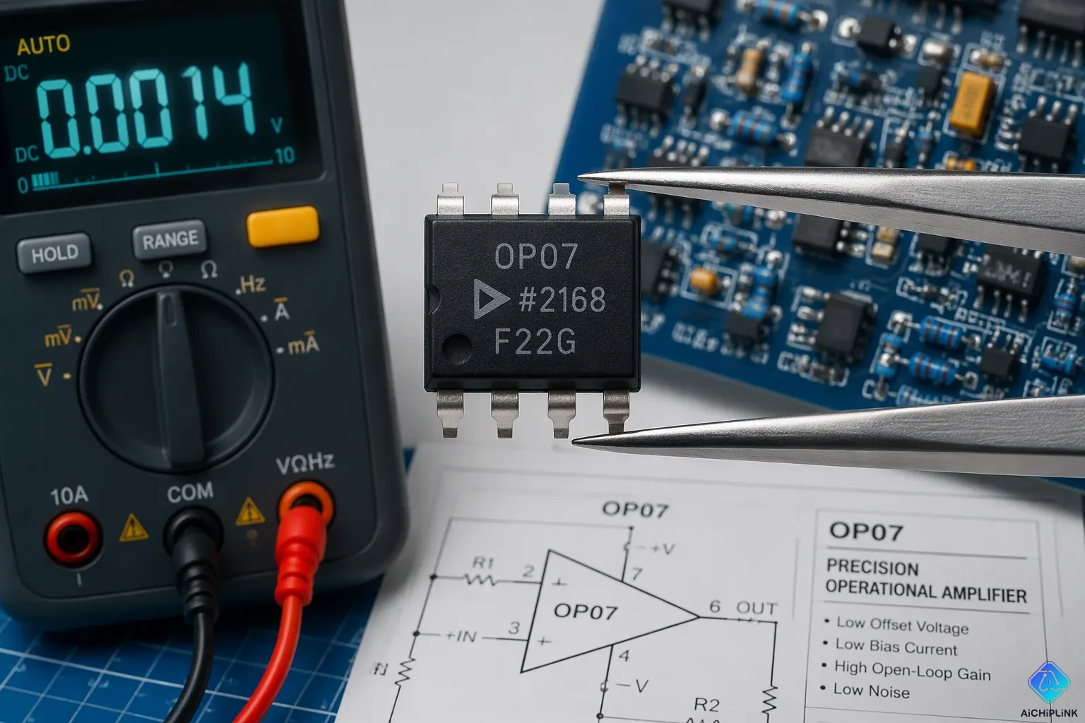
The OP07 is an ultra-low offset voltage op-amp IC. Designers depend on it for precise signal conditioning in DC-coupled systems. Its input offset voltage is the small difference in voltage a circuit needs at its inputs to make the output zero. Any gain stage multiplies that error along with the signal. So a tiny input offset can turn into a large output error. The OP07 keeps this error very small, which makes the operational amplifier a reliable choice for accurate measurement chains. The article explains how the device works, lists its key features, and shows the pinout, applications, and practical usage.
Key Takeaways
-
The OP07 op-amp keeps input offset voltage very low, which means less error in precise signal chains.
-
The OP07E grade has a maximum offset of 75 μV and drift near 0.2 μV/°C, so it often needs no external adjustment.
-
Use the OP07 for slow, accurate DC signals; choose the OP27 for speed or the OP77 for low power.
-
Connect power supplies within ±3 V to ±18 V and leave headroom for the output swing.
-
Read the datasheet before finalizing your design to check limits, packages, and layout guidance.
What Is the OP07 Operational Amplifier?
Definition and Primary Function
The OP07 is a low-noise bipolar op-amp IC that does not use chopper stabilization. It usually runs on a dual power supply. Designers use this op-amp for DC-accurate signal chains. The device does not use chopping or auto-zeroing to fix errors. Instead, it gets its low offset voltage from careful manufacturing. This makes the OP07 a steady precision op-amp IC for measurement and instrumentation work.
The main job of the OP07 is to amplify small differential signals with very little added error. A differential amplifier circuit built around this op-amp can boost a sensor output while keeping the error floor low. The amplifier also gives high open-loop gain and good common-mode rejection. These traits help keep slowly changing DC signals precise.
How the OP07 Works
Manufacturers get the ultra-low offset voltage op-amp behavior by trimming at the wafer stage. During production, they adjust each die so the input offset voltage drops to a very small value. Input offset voltage is the differential voltage needed at the inputs to make the output zero. A smaller value means less error at the output after gain.
Texas Instruments lists the OP07 maximum input offset voltage at 25°C as 0.15 mV. That number applies to the standard grade. The OP07E grade tightens the limit even more, and it often removes the need for external nulling. The offset also stays small over temperature, which helps long-term accuracy in DC-coupled designs.
The OP07 compares well against other precision parts. Texas Instruments notes that the OPA202 offers 0.2 mV offset with lower power and lower voltage noise at 1 kHz. The TLV07 uses CMOS inputs and aims for better AC performance. Each part fits a different design goal. The OP07 is still a strong choice when low offset voltage and low drift matter most.
EEVblog forum members have compared offset values across several precision op-amps. Their table lists the LMC662 at 3 mV, the AD795 at about -100 µV, the AD706 at +30 µV, the AD542 at 250 µV, and the LM11 at 100 µV. The same discussion shows a bar chart of these offset voltages.
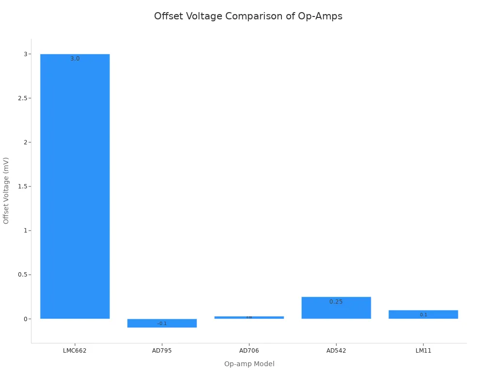
These comparisons show why the OP07 earns its place in precision work. Its trimmed offset sits at the low end of the group. The bipolar input stage also keeps input bias current moderate and predictable. A designer can therefore build a differential amplifier with confidence in its DC behavior. The next sections cover the key specifications and the pinout.
Key Features of the Ultra-low Offset Voltage Op-Amp IC

Offset Voltage and Drift
The main spec of this ultra-low offset voltage op-amp IC is its trimmed input offset voltage. The OP07E grade keeps a maximum input offset voltage of 75 μV at room temperature. That number usually means most designs do not need external nulling. A builder can wire the operational amplifier into a gain stage and trust the output to stay close to zero with no input signal.
Drift matters just as much as the starting offset. The OP07 keeps offset drift near 1.3 μV/°C across its operating range. A small drift number protects accuracy in circuits that run warm or sit in rooms with changing temperatures. Temperature stability of this order lets a precision differential amplifier hold its calibration over long periods. The offset stays predictable, so a designer spends less time on recalibration routines.
Noise, Slew Rate, and Gain
The table below collects the main specifications of the ultra-low offset voltage op-amp.
| Parameter | Specification |
|---|---|
| Maximum input offset voltage (OP07E) | 75 μV |
| Offset drift | 1.3 μV/°C |
| Slew rate (Analog Devices OP07) | ~0.3 V/µs |
| Slew rate (STMicroelectronics OP07) | ~0.17 V/µs |
| Supply capability | 18 V |
| Power dissipation | 120 mW |
| Input voltage range | Wide |
| Common-mode rejection ratio | High |
Slew rate differs by vendor. Analog Devices rates its OP07 at about 0.3 V/µs, and STMicroelectronics lists roughly 0.17 V/µs. A drunk-beaver.rocks comparison places the LM308 at about 0.3 V/µs typical and notes that the OP07 has slightly more open-loop gain than the LM308. High open-loop gain supports high voltage gain in closed-loop stages. The same comparison shows the two parts trading blows on speed, so the OP07 suits slow, accurate work better than fast switching duty.
The wide input voltage range and high common-mode rejection ratio complete the picture. A high common-mode rejection ratio lets the differential amplifier circuit ignore noise that appears on both inputs. Input bias current stays moderate and predictable, which keeps error budgets simple. The 18 V supply capability and 120 mW power dissipation set the practical operating limits. Designers should respect both figures when they plan supply rails and thermal headroom. The op-amp delivers its best behavior inside those bounds.
Pin Configuration and Offset Nulling
Pin Functions
The 8-pin PDIP package gives the OP07 a simple, standard layout. The pin configuration description below shows what each pin does.
| Pin Number | Pin Name | Description |
|---|---|---|
| 1, 8 | VOS Trim | Used to set offset voltage if required |
| 2 | Inverting Input (IN-) | The inverting pin of the op-amp |
| 3 | Non-Inverting Input (IN+) | The non-inverting pin of the op-amp |
| 4 | V- | Connected to negative rail or ground |
| 5 | NC | Not connected |
| 6 | Output | Output pin of the op-amp |
| 7 | V+ | Connected to the positive rail of supply voltage |
Pins 2 and 3 are the two inputs of the operational amplifier, and pin 6 sends out the output. Pins 4 and 7 connect to the power supply rails. Pin 5 has no internal connection, so a designer just leaves it open. The two input offset pins sit at opposite corners of the package, which keeps a trimmer away from the signal path.
Using the Offset Null Pins
A trimmer placed between pins 1 and 8 does offset nulling when a design needs it. According to EEVblog, the TI datasheet gives a nulling range of 4 mV for the trimmer. Trimming off a small value like 50 µV with a 10-turn trimmer and no padding resistors is a tricky job. Fixed precision resistors can limit the trim range, or they can take the place of the trimmer entirely.
The OP07E grade often needs no external nulling at all. Its 75 µV maximum input offset voltage usually keeps the output error small enough for the application. EEVblog notes that well-designed bipolar input parts null their temperature coefficient of input offset voltage when their input offset voltage is nulled. That trait makes offset voltage adjustment a useful tool for demanding work. During the trim, a designer should ground the input through a low source resistance and avoid shorting the input pins together, since the operational amplifier would then saturate at one rail.
Applications of the Ultra-low Offset Voltage Op-Amp
Precision Sensor Signal Conditioning
A pressure-sensor amplifier that feeds a microcontroller shows where this ultra-low offset voltage op-amp works best. Best Engineering Projects describes a working chain built around the OP07. The first stage boosts the sensor signal 100 times, and a 1 MΩ resistor and a 10 kΩ resistor set the gain. A CD4052 multiplexer then picks among several sensor inputs. A second OP07 works as a buffer, and two more stages make complementary outputs that stand up to noise on long cable runs.
The low offset voltage of the part keeps that chain accurate. Allelcoelec notes a maximum offset of 150 µV and input currents as low as 1.8 nA, which help hold readings steady in sensitive measurement work. The same source lists strain gauge bridges, RTDs, and thermocouples as good fits. A designer who builds a differential amplifier circuit for an ADC front end gets a clean signal with little added error.
The right fit depends on the job. The OP27 suits designs that need more speed and lower noise. The OP77 draws less quiescent current, so portable products may prefer it. The OP07 stays a solid pick when DC precision is the top priority.
Low-drift DC Amplification
Slow DC signals do best with a stable amplifier. Allelcoelec lists the OP07 offset at just 75 µV and drift at only 1.3 µV/°C. The input voltage range reaches ±14 V, and supply voltages run from ±3 V to ±18 V. Noise sits at 0.6 µV peak-to-peak. IC Components adds an input bias current of ±2 nA and an open-loop gain of 300 V/mV. That mix supports high voltage gain without drift spoiling the result.
A differential amplifier built on these numbers holds its calibration through temperature swings. The operational amplifier needs less nulling, which makes the design simpler. The operational amplifier also keeps error risks low in complex circuits. An instrumentation amplifier front end gains from the same traits. The operational amplifier gives steady performance from -65°C to +125°C. Designers who need clean signal integrity in a precision DC path will find the part well suited to the task.
Circuit Design and Packages
Supply Voltage and Output Limits
Most designs use a dual supply for the OP07. The part takes rails from ±3 V to ±18 V, and the 18 V number is the total supply limit. A designer chooses rails that leave room for the signal to swing. The output voltage cannot reach the rails, so a stage that must deliver a big swing needs headroom above and below the signal. Keep the 120 mW power dissipation limit in mind when the amplifier drives a heavy load.
A simple precision stage shows the idea. Set the operational amplifier in a non-inverting gain of 100 with a 1 MΩ feedback resistor and a 10 kΩ ground resistor. The 75 µV maximum offset of the OP07E grade then shows up as a small output error, and the low drift keeps that error steady as the board warms. Check the input voltage range against the common-mode level of the source before you fix the rails.
Packages and Equivalents
The 8-pin PDIP is still the classic package for this op-amp, and through-hole parts work well on breadboards and older boards. Surface-mount options exist for compact layouts. A designer should confirm the exact package list in the datasheet before committing a footprint.
Several parts cover nearby ground. The OP27 targets faster, lower-noise work, and the OP77 draws less quiescent current. The OPA202 and TLV07 offer their own trade-offs in power and AC behavior. Each option fits a different design goal, and the OP07 holds its place where DC accuracy leads. A differential amplifier circuit built on any of them needs a careful check of the final numbers. Read the datasheet for limits, derating, and layout guidance before the design goes to production.
The OP07 is still a trusted precision op-amp for designs that need DC accuracy. Trimming at the wafer stage keeps its offset voltage at 75 μV maximum in the OP07E grade. Low drift keeps that number steady as temperature changes. These traits make the operational amplifier a great fit for slow, accurate signal chains.
The job decides the choice. The OP07 puts DC accuracy first. The OP27 handles faster, lower-noise work. The OP77 uses less current for portable products. Each operational amplifier fits its own job.
A designer should read the datasheet before finalizing any stage. It lists the limits, derating rules, and layout guidance that a differential amplifier needs. The operational amplifier rewards careful planning with stable, predictable behavior.

Written by Jack Elliott from AIChipLink.
AIChipLink, one of the fastest-growing global independent electronic components distributors in the world, offers millions of products from thousands of manufacturers, and many of our in-stock parts is available to ship same day.
We mainly source and distribute integrated circuit (IC) products of brands such as Broadcom, Microchip, Texas Instruments, Infineon, NXP, Analog Devices, Qualcomm, Intel, etc., which are widely used in communication & network, telecom, industrial control, new energy and automotive electronics.
Empowered by AI, Linked to the Future. Get started on AIChipLink and submit your RFQ online today!
Frequently Asked Questions
Does the OP07E grade need external offset nulling?
Most designs don't need it. The OP07E grade keeps a maximum input offset voltage of 75 μV at room temperature. That small error usually keeps the output close enough to zero. A designer adds a trimmer between pins 1 and 8 only when the application needs tighter accuracy.
How does the OP07 differ from the OP27 and OP77?
Each part serves a different goal. The OP27 is made for faster, lower-noise work. The OP77 draws less quiescent current, so portable products may like it better. The OP07 puts DC accuracy first. A precision differential amplifier stage benefits from its trimmed offset and low drift.
What supply rails does the OP07 accept?
The part runs on a dual supply from ±3 V to ±18 V. The 18 V figure is the total supply limit. A designer picks rails that leave headroom for the output swing. The output can't reach the rails, so the signal needs room above and below.
Why does offset drift matter in a DC amplifier?
Drift keeps the starting offset steady as the board warms. The OP07 holds offset drift near 1.3 μV/°C. A stable number protects calibration over long periods. The operational amplifier then needs less frequent recalibration in temperature-changing environments.
Which package should a designer choose?
The 8-pin PDIP works well on breadboards and older boards. Surface-mount options exist for compact layouts. A designer should confirm the exact package list in the datasheet before committing a footprint. The operational amplifier works the same way in either package.