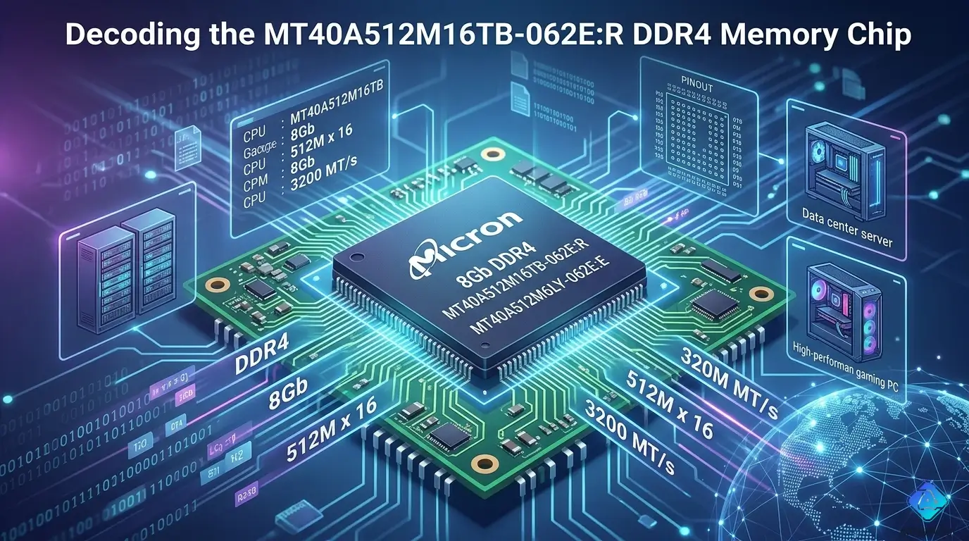
MT40A512M16TB-062E:R: Why "512M" Is Not 512 Megabytes — and What the Colon Before "R" Actually Means
Two elements of the MT40A512M16TB-062E:R part number routinely cause confusion, and both involve the same underlying issue: reading familiar-looking notation and assuming it maps to familiar meanings.
The first: 512M does not mean 512 megabytes. In Micron's DDR4 DRAM naming convention, "512M" is the row address space — 512 mega-locations, each 16 bits wide (the x16 designation). Total capacity is 512M × 16 bits = 8,192 megabits = 8 Gb = 1 gigabyte per chip. A designer who sees "512M" and infers 512 MB will arrive at a system memory calculation that is exactly half of the correct value — potentially specifying twice as many chips as needed, or understating available memory by half.
The second: the colon in ":R" is not punctuation — it is a field delimiter in Micron's part number structure. The ":R" is a separate suffix field encoding the packaging format — Tape-and-Reel. Micron uses a colon to separate the device specification part of the number from the packaging/reel specification. This is why you will see the same device listed as MT40A512M16TB-062E (tray) and MT40A512M16TB-062E:R (tape-and-reel) — identical silicon, different packaging. The industrial temperature variant is MT40A512M16TB-062E**-IT**:R, where "-IT" indicates the −40°C to +85°C temperature range.
Getting these two fields right — capacity per chip and packaging format — is the starting point for correctly specifying MT40A512M16TB-062E:R in a bill of materials.
1.0 Part Number Decoded: MT40A512M16TB-062E:R Field by Field
Micron's DDR4 SDRAM component part numbers follow a structured format. The colon separating the main number from the packaging suffix is a Micron-specific notation that some engineers encounter as unexpected:
MT — Micron Technology product prefix
40A — DDR4 SDRAM component code:
- 4 = DDR4 generation (Micron uses 4 for DDR4)
- 0A = component type sub-code for standard DDR4 SDRAM die
512M — Row address space: 512 Meg (512 × 2²⁰ = 536,870,912 locations) This is NOT 512 megabytes. It is 512M addressable locations, each holding 16 bits (for the x16 variant). Total bit capacity = 512M × 16 = 8 Gb = 1 GB per chip.
16 — Data bus width: x16 — the chip presents 16 data lines (DQ0–DQ15)
T — Die technology generation code within Micron's DDR4 lineup. T indicates a specific manufacturing process node generation for this die family.
B — Die version: B = second silicon generation within the T-process family (Micron's "B-die" for this generation of DDR4)
-062 — Speed grade encoding:
- This encodes tCK(min) = 0.625 ns — the minimum clock cycle time
- tCK = 0.625 ns → clock frequency = 1/0.625 ns = 1600 MHz
- DDR4 data rate = 2 × clock = 3200 MT/s = DDR4-3200 (PC4-25600)
- The "062" encodes the last three significant digits of the tCK value: 0.625 ns
E — Die revision within the B-generation:
- E = fifth revision of the B-die silicon for this speed grade combination
- Silicon revisions progress alphabetically (A, B, C, D, E...) as Micron makes incremental improvements
:R — Packaging format (Tape-and-Reel):
- The colon ":" is Micron's field delimiter between the device specification and the packaging specification
- R = Tape-and-Reel packaging (standard 3,000-unit or 4,000-unit reel for production assembly)
- Without the :R suffix (MT40A512M16TB-062E alone) = Tray packaging
- -IT:R variant = same device, industrial temperature range (−40°C to +85°C), tape-and-reel
Temperature grade of the base part (no -IT suffix): The MT40A512M16TB-062E:R without the "-IT" designation is the commercial temperature grade: operating range 0°C to +95°C TC (case temperature). Note: DDR4 DRAM uses TC (case/junction temperature), not ambient.
2.0 Specifications and What They Mean in Practice
From Micron's MT40A512M16TB datasheet (Micron Document #: TN-46-16):
Capacity and organization:
- Total capacity: 8 Gb = 1 GB per chip
- Organization: 512M × 16 (512M addressable row locations × 16 data bits)
- Internal bank structure (x16): 8 banks (for x16 configuration — contrast with x4/x8 which have 16 banks)
- Bank Groups: 2 (DDR4 architecture: 2 bank groups × 4 banks each = 8 banks total for x16)
- Row addresses: A[0:14] = 15 bits = 32,768 rows per bank
- Column addresses: A[0:9] = 10 bits = 1,024 columns per row
Speed grade (-062E = DDR4-3200):
- tCK(min): 0.625 ns
- Data rate: 3200 MT/s
- Clock frequency: 1600 MHz
- CAS Latency at DDR4-3200: CL21
- tRCD: 21 cycles (13.125 ns)
- tRP: 21 cycles (13.125 ns)
- tRAS: 47 cycles (29.375 ns minimum)
- Absolute CAS latency: 21 × 0.625 ns = 13.125 ns
Comparison: DDR4-2133 CL15 gives 15 × 0.9375 = 14.06 ns absolute latency. DDR4-3200 CL21 gives 13.125 ns — actually lower absolute latency at higher speed.
Interface:
- DQ bus: 16 bits (DQ0–DQ15)
- Data strobes: UDQS_t/UDQS_c (upper byte, DQ8–DQ15) and LDQS_t/LDQS_c (lower byte, DQ0–DQ7) — differential pairs
- DM/DBI: 2 data mask/data bus inversion pins (UDM, LDM)
- Clock: CK_t / CK_c — single differential clock pair
- ODT: On-Die Termination, independently programmable RTT_NOM, RTT_WR, RTT_PARK
Power:
- VDD / VDDQ: 1.2V (1.14V–1.26V)
- VPP: 2.5V (required, separate from VDD)
- IDD4R (peak read current, DDR4-3200): ~180–230 mA per chip
Package:
- 96-ball FBGA (Fine-pitch BGA), body 9mm × 9mm (Z41C package code in some listings)
- Ball pitch: 0.8mm
- MSL: MSL-3 (moisture sensitivity level 3)
3.0 How DDR4 8n-Prefetch Works and Why x16 Matters
The 8n-prefetch architecture:
DDR4 uses an 8n-prefetch scheme: for every read or write operation, the DRAM internally accesses 8n bits from the memory array in a single access cycle, where n is the data bus width. For the x16 device: 8 × 16 = 128 bits = 16 bytes are fetched from the array per command. This 16-byte block is then serialized onto the 16-bit external DQ bus over 8 half-clock periods (using DDR double-edge clocking, 4 full clock cycles).
This prefetch architecture is why DDR4 can achieve high data rates (3200 MT/s) while the internal DRAM array itself operates at a much slower clock frequency: internal array frequency = external clock / 8 = 1600 MHz / 8 = 200 MHz. The DRAM's sense amplifiers and array cells operate at 200 MHz; the external bus bursts at 1600 MHz. This internal/external frequency ratio is the fundamental speed-scaling mechanism of all modern DRAM.
Why the x16 organization has 8 banks instead of 16:
DDR4 x4 and x8 devices have 16 banks (4 bank groups × 4 banks). DDR4 x16 devices have only 8 banks (2 bank groups × 4 banks). This is an architectural trade-off: x16 devices have wider data buses per chip (more parallel data), so fewer chips are needed to build a given bus width — but the reduced bank count means slightly less bank-level parallelism for random access workloads. For most embedded applications with relatively sequential access patterns, the 8-bank x16 configuration is fully adequate.
Building a 32-bit DDR4 interface with x16 chips:
Many embedded SoCs (NXP i.MX8, Rockchip RK3568, Allwinner H6) implement 32-bit DDR4 interfaces. One x16 chip provides 16 bits. Two x16 chips provide 32 bits. Two MT40A512M16TB-062E:R chips in a 32-bit single-rank configuration provide:
2 chips × 1 GB = 2 GB total, 32-bit bus width, at DDR4-3200 data rate.
Peak bandwidth = 3200 MT/s × 4 bytes (32-bit) = 12.8 GB/s
This is the most common embedded application for this chip — two chips providing 2 GB on a 32-bit DDR4 interface to an ARM application processor.
4.0 ⚠️ Four Design Pitfalls with MT40A512M16TB-062E:R
Pitfall 1: Confusing 512M (row address space) with 512 MB (capacity)
This is the opening hook of this article and the most consequential error. The "512M" in MT40A512M16TB designates 512 mega-addressable locations at x16 data width. Total capacity = 512M × 16 / 8 = 1 GB per chip. BOM calculations that read "512M" as "512 MB" will specify twice as many chips as needed (to reach the target capacity) or underestimate available memory by 2×. Always convert explicitly: density (Mb) = 512M × 16 = 8,192 Mb = 8 Gb = 1 GB.
Pitfall 2: Ordering MT40A512M16TB-062E (tray) when production requires :R (tape-and-reel)
The MT40A512M16TB-062E (without :R) is tray-packaged, suitable for engineering samples and small manual assembly. The MT40A512M16TB-062E:R is tape-and-reel, required for high-speed automated PCB assembly (pick-and-place machines require T&R for reliable component feeding). Ordering tray for a production run results in either manual placement (not feasible at volume) or a procurement delay to convert to T&R packaging. Specify :R for any production-intent design from the outset. The industrial temperature variant is MT40A512M16TB-062E**-IT**:R — verify the temperature grade matches the deployment environment before finalizing the BOM.
Pitfall 3: Omitting the VPP 2.5V supply rail
DDR4 requires VPP = 2.5V in addition to VDD/VDDQ = 1.2V. VPP powers the wordline boosting circuit inside the DRAM array and must be present and stable before VDD/VDDQ power up (power sequencing requirement: VPP first, then VDD). A design ported from DDR3 to DDR4 that does not add the VPP rail will result in a device that does not initialize — and the symptom (no memory response) is easily confused with a signal integrity or controller initialization problem. If the PCB has no 2.5V rail from another source, add a small LDO or charge pump generating 2.5V specifically for VPP.
Pitfall 4: Using default DDR4 controller settings without accounting for DDR4-3200 timing requirements
DDR4-3200 is among the highest standard DDR4 speeds. At tCK = 0.625 ns, the setup and hold timing margins are tight. PCB trace length mismatch on DQ/DQS pairs beyond ±25 ps (approximately ±3 mm on FR4), or failure to use the controller's DQ-DQS training algorithms, will result in marginal bit errors that are temperature-dependent and difficult to reproduce. Always enable the memory controller's DDR4 training sequence (ZQ calibration, write leveling, read/write DQ-DQS training) and verify training completion before declaring the design functional. Random bit errors in DDR4-3200 designs that pass at room temperature but fail at elevated temperature are almost always traced to insufficient DQ-DQS alignment margin.
5.0 Application Design Notes: PCB Layout, Power, and Controller Init
Power supply sequencing:
DDR4 power-up sequence: VPP (2.5V) must reach operating range before VDD (1.2V) and VDDQ (1.2V). Use a power sequencing circuit or cascaded LDO arrangement. After VDD and VDDQ are stable, RESET# must be held low for ≥ 200 µs before the initialization sequence begins.
Decoupling:
Place 100 nF X5R/X7R ceramic capacitors within 2 mm of every VDD and VDDQ ball on each chip. Add 4.7–10 µF bulk per chip per supply domain. For VPP, place 100 nF per VPP ball. Inadequate decoupling on VDDQ (the data bus supply) produces noise on DQ/DQS signals that manifests as training failures at DDR4-3200.
PCB trace routing (32-bit interface, 2 chips):
| Signal group | Impedance | Match tolerance |
|---|---|---|
| CK_t / CK_c | 85–100 Ω differential | Within pair: ±5 mil |
| DQS_t / DQS_c (per byte) | 85–100 Ω differential | Within pair: ±5 mil |
| DQ per byte lane | 40–50 Ω single-ended | Within byte lane: ±15 ps |
| Address / Command | 40–50 Ω single-ended | ±50 ps |
ZQ calibration resistor:
Connect a 240 Ω (±1%) resistor from the ZQ pin to ground on each chip. This resistor provides the reference for the chip's on-die output impedance calibration. Incorrect value or long trace reduces calibration accuracy, degrading signal integrity at DDR4-3200.
Controller initialization:
The DDR4 initialization sequence after RESET# deasserts:
- CKE high after tXPR from RESET# deassertion
- Mode register writes (MR2, MR3, MR1, MR0 in order)
- ZQ Calibration Long (ZQCL)
- Write leveling enable/disable
- DQ-DQS training (if controller supports)
6.0 Variant Comparison: :R vs Tray, IT vs Standard, 062 vs Other Speed Grades
Packaging variants (same die):
| Part number | Packaging | Use case |
|---|---|---|
| MT40A512M16TB-062E | Tray | Engineering samples, manual assembly |
| MT40A512M16TB-062E:R | Tape-and-Reel | Production assembly (this part) |
Temperature variants:
| Part number | Temperature | Junction range |
|---|---|---|
| MT40A512M16TB-062E:R | Commercial | 0°C to +95°C TC |
| MT40A512M16TB-062E-IT:R | Industrial | −40°C to +85°C TC |
Note: the commercial grade's upper limit is +95°C TC — higher than many competing DDR4 devices at +85°C. Micron specifies TC (case temperature), and the 95°C upper bound provides more thermal headroom for high-activity embedded applications.
Speed grade variants (same 512M × 16 die):
| Speed suffix | tCK(min) | Data rate | CL | Availability |
|---|---|---|---|---|
| -075 | 0.75 ns | DDR4-2666 | 19 | Wide |
| -062E | 0.625 ns | DDR4-3200 | 21 | Standard |
| -062E:R | 0.625 ns | DDR4-3200 | 21 | T&R production |
A -075 part can be used where -062E is specified (slower speed grade in a faster controller will operate at the slower rate). A -062E cannot substitute for a -075 in a system qualified only for DDR4-2666 — though the -062E will operate correctly at DDR4-2666, the system qualification must cover the actual installed component.
7.0 Sourcing MT40A512M16TB-062E:R
The MT40A512M16TB-062E:R is an active Micron production part available from authorized distributors including DigiKey, Mouser, Arrow, and Avnet. Micron directly authorizes these channels for production-volume DRAM sales. Pricing at distributor quantity: approximately $3–7 per unit at 1–1,000 piece quantities; lower at production volume direct pricing.
MSL-3 storage requirement: The FBGA-96 package is rated MSL-3 (Moisture Sensitivity Level 3). Parts must be stored in sealed dry-pack packaging at ≤ 30°C / 60% RH. If the dry-pack seal is broken and the parts are not used within 168 hours at ambient conditions, a bake-out (≥ 120°C for 5 hours per JEDEC J-STD-020) is required before reflow assembly to prevent delamination from moisture-induced steam pressure.
Counterfeit risk: Micron DDR4 chips are counterfeited, particularly in the secondary market at below-market pricing. Common approaches include remarking lower-density or lower-speed grade devices. Verification: read the DRAM's mode register to confirm device density code and manufacturer ID. DDR4 MR8 (Mode Register 8) contains the manufacturer ID code — genuine Micron parts return Micron's JEDEC-assigned manufacturer ID (2C hex). Address-aliasing functional test (write pattern to all 1 GB of addresses, read back) detects density counterfeits.
For verified authentic Micron MT40A512M16TB-062E:R with competitive pricing and traceability, visit aichiplink.com.
8.0 Real Questions from Embedded Hardware Designers
Q: I am using two MT40A512M16TB-062E:R chips for a 32-bit DDR4 interface on an NXP i.MX8M Plus. My training logs show DQ-DQS alignment failing intermittently on one byte lane. What are the likely causes?
A: Intermittent DQ-DQS training failures on a single byte lane — especially if they are temperature-dependent — indicate marginal setup/hold timing. Most likely causes in order: (1) DQ trace length mismatch within the failing byte lane — traces in the same byte lane should be matched within ±15 ps (≈ ±2–3 mm on FR4). Measure the PCB traces and compare against the design intent. (2) Insufficient VDDQ decoupling near the chip — noise on VDDQ directly degrades DQS signal quality. Add or replace decoupling capacitors closer to the VDDQ balls of the failing chip. (3) ZQ resistor value or placement — a 240 Ω ZQ resistor with more than 10 mm of trace to the DRAM or a tolerance wider than ±1% will produce suboptimal ODT calibration, worsening DQ/DQS margins. Check your ZQ resistor placement and tolerance. (4) If failures correlate with temperature rise, the issue may be thermal: MT40A512M16TB-062E:R's FBGA-96 package has limited self-heating capability — if adjacent components heat the DRAM above 90°C case temperature, timing parameters shift toward their limits.
Q: Can MT40A512M16TB-062E:R be run at DDR4-2400 instead of DDR4-3200 to improve stability in a challenging PCB layout?
A: Yes. A DDR4-3200 rated chip (tCK(min) = 0.625 ns) can be initialized and operated at any lower standard data rate: DDR4-2400 (tCK = 0.833 ns), DDR4-2133, or any lower speed. Operating below the chip's rated maximum speed provides additional timing margin — setup/hold requirements scale with tCK, so at DDR4-2400 the timing budget is 33% larger per cycle than at DDR4-3200. For a difficult PCB layout where trace length matching is imperfect or signal integrity simulation shows marginal margins at DDR4-3200, running at DDR4-2400 or DDR4-2666 trades peak bandwidth for reliability. Configure the memory controller for the lower speed grade and initialize the DRAM with the appropriate mode register timing parameters for that speed.
Q: What is the difference between MT40A512M16TB-062E:R and MT40A1G8SA-075:R? They seem to be from the same Micron DDR4 family.
A: Both are 8Gb DDR4 devices from Micron's MT40A family, but with different organizations and speed grades. MT40A512M16TB = 512M × 16 (x16, 8Gb total), DDR4-3200. MT40A1G8SA = 1G × 8 (x8, 8Gb total), DDR4-2666 (-075 speed grade). Same total capacity (8Gb = 1GB per chip), but different data bus width and speed. The x16 (512M × 16) device has 16 DQ pins per chip and half the chip count needed for a given bus width compared to x8. The x8 (1G × 8) device has 8 DQ pins per chip and needs twice as many chips for the same bus width, but offers more bank-level parallelism (16 banks in x8 vs 8 banks in x16) for random-access workloads. For a 32-bit interface: 2 × x16 chips vs 4 × x8 chips — same memory capacity, different chip count and PCB routing complexity.
9.0 Quick Reference Card
Part Number Decode:
| Field | Value | Meaning |
|---|---|---|
| MT40A | MT40A | Micron DDR4 SDRAM |
| 512M | 512M | 512M row locations × 16b = 8Gb = 1GB |
| 16 | 16 | x16 data bus (16 DQ pins) |
| TB | TB | Die technology + generation |
| -062 | -062 | tCK = 0.625 ns → DDR4-3200 |
| E | E | Die revision E |
| :R | :R | Tape-and-Reel packaging (colon = field delimiter) |
The Critical Calculation:
512M locations × 16 bits/location = 8,192 Mb ÷ 8 = 1 GB per chip
Key Specifications:
| Parameter | Value |
|---|---|
| Capacity per chip | 1 GB (8 Gb) |
| Data rate | DDR4-3200 (3200 MT/s) |
| tCK(min) | 0.625 ns |
| CAS Latency | CL21 at DDR4-3200 |
| Absolute tCL | 13.125 ns |
| VDD / VDDQ | 1.2V |
| VPP | 2.5V (required) |
| Banks (x16 config) | 8 (2 bank groups × 4 banks) |
| Package | FBGA-96, 9×9mm, 0.8mm pitch |
| Temperature | 0°C to +95°C TC (commercial) |
Packaging Variants:
| Suffix | Package | Use case |
|---|---|---|
| (none) | Tray | Engineering/low-volume |
| :R | Tape-and-Reel | Production assembly |
| -IT:R | T&R, industrial | −40°C to +85°C TC |
32-bit Interface with 2 chips: 2 × MT40A512M16TB-062E:R → 2 GB total, 32-bit DDR4-3200 = 12.8 GB/s peak BW
For sourcing Micron MT40A512M16TB-062E:R with verified authenticity and competitive pricing, visit aichiplink.com.

Written by Jack Elliott from AIChipLink.
AIChipLink, one of the fastest-growing global independent electronic components distributors in the world, offers millions of products from thousands of manufacturers, and many of our in-stock parts is available to ship same day.
We mainly source and distribute integrated circuit (IC) products of brands such as Broadcom, Microchip, Texas Instruments, Infineon, NXP, Analog Devices, Qualcomm, Intel, etc., which are widely used in communication & network, telecom, industrial control, new energy and automotive electronics.
Empowered by AI, Linked to the Future. Get started on AIChipLink and submit your RFQ online today!
Frequently Asked Questions
What does “512M” mean in MT40A512M16TB-062E:R?
“512M” refers to 512 mega-addressable memory locations, not 512MB capacity. Because this is a x16 DDR4 device, total density is 512M × 16 bits = 8Gb, which equals 1GB per chip, making it suitable for embedded 32-bit and 64-bit DDR4 memory designs.
What does the “:R” suffix mean?
The :R suffix indicates tape-and-reel packaging for automated SMT production. The colon is Micron’s packaging field delimiter, separating the device specification from assembly packaging information. The silicon is identical to tray-packaged versions.
Can MT40A512M16TB-062E:R run below DDR4-3200?
Yes. Although rated for DDR4-3200 (3200 MT/s), the chip can operate at lower JEDEC speeds such as DDR4-2666 or DDR4-2400, which often improves timing margin and signal integrity for challenging PCB layouts.
Why is VPP required for this DDR4 chip?
Unlike DDR3, DDR4 requires a dedicated 2.5V VPP rail to power internal wordline boosting circuits. Without VPP, the DRAM will fail initialization even if VDD and VDDQ are correctly supplied at 1.2V.
How much memory do two MT40A512M16TB-062E:R chips provide?
Two chips in a 32-bit DDR4 interface provide 2GB total capacity and deliver up to 12.8 GB/s peak bandwidth at DDR4-3200, making this configuration common in embedded systems using processors like NXP i.MX8 and similar ARM SoCs.