Open a bill of materials from any high-volume consumer electronics product built in the last five years and look at the 128Mbit SPI flash component. There is a reasonable chance the manufacturer approved a W25Q128 but built the production run with a GD25Q128. Not because they did anything wrong — GigaDevice's GD25Q128 is a legitimate, well-specified part that appears on the approved vendor lists of hundreds of product families worldwide. The problem is that a surprising number of firmware engineers do not find out about this substitution until their Quad SPI driver fails QA at a factory they have never visited.
This guide covers everything you need about the GD25Q128 — specifications, variant decoder, JEDEC ID, register map, compatibility with the W25Q128, the specific pitfalls that catch engineers off guard, and how to write firmware that works correctly regardless of which 128Mbit flash ends up on the board.
1.0 What Is the GD25Q128?
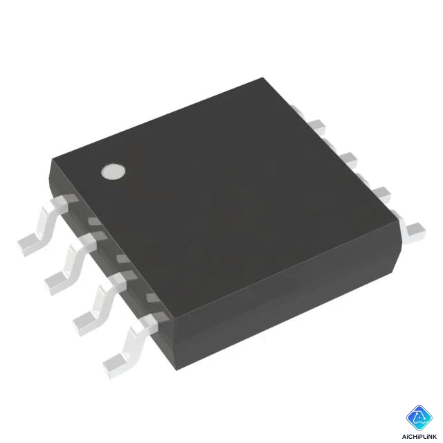
The GD25Q128 is GigaDevice Semiconductor's 128 Mbit (16 MB) SPI NOR Flash memory. It is the direct equivalent of the Winbond W25Q128 and Macronix MX25L12835F in terms of capacity and interface — same 8-pin SOIC package, same 4KB sector / 64KB block layout, same standard SPI / Dual SPI / Quad SPI command set, same 2.7V–3.6V supply.
GigaDevice is a Chinese semiconductor company founded in 2005 and now one of the world's top five SPI NOR Flash producers by volume. The GD25Q128 in particular is one of the most widely shipped 128Mbit NOR Flash components in the world by unit count — which is why it shows up as a substitute on so many production boards.
What makes the GD25Q128 different from its Winbond and Macronix equivalents is not the hardware — the pinout is identical and the electrical interface is compatible — but the JEDEC manufacturer ID (0xC8) and a small number of status register details that affect Quad SPI initialization. Get those two things right in firmware and the GD25Q128 is a straightforward, reliable component. Miss them and you will spend a day debugging a Quad SPI bus that works fine on the bench with Winbond parts but fails intermittently on production boards that shipped with GigaDevice.
2.0 Part Number Decoder: Which GD25Q128 Do You Actually Have?
GigaDevice uses a structured part number system. Here is how to read a GD25Q128 part number:
GD 25 Q 128 E S I G R
- GD — GigaDevice manufacturer prefix
- 25 — SPI Flash product family
- Q — 3.3V voltage series (Q = 2.7V–3.6V; L = 1.65V–2.0V; B = wide voltage)
- 128 — Density: 128 Mbit (16 MB)
- E — Silicon revision (E = current production; C = previous generation)
- S — Package: S = SOP-8; W = WSON; U = USON; D = DIP-8
- I — Temperature: I = Industrial −40°C to +85°C
- G — RoHS compliant / Pb-free
- R — Tape-and-reel (omitted for tube)
Current production GD25Q128 variants (3.3V):
| Part Number | Package | Packaging | Notes |
|---|---|---|---|
| GD25Q128ESIGR | SOP-8 | Tape & Reel | Current standard; most common |
| GD25Q128ESIG | SOP-8 | Tube | Same die, tray |
| GD25Q128EWIGR | WSON 5×6 | Tape & Reel | Smaller SMD footprint |
| GD25Q128EYIGR | WSON 8×6 | Tape & Reel | Larger WSON |
| GD25Q128CSIG | SOP-8 | Tube | Previous C revision; still common |
1.8V equivalent (GD25LQ128 — not interchangeable with GD25Q128):
| Part Number | VCC | Package |
|---|---|---|
| GD25LQ128DSIGR | 1.65V – 2.0V | SOP-8 |
| GD25LQ128EWIGR | 1.65V – 2.0V | WSON |
Critical warning: The Q-series (3.3V) and L-series (1.8V) variants are pin-compatible but not voltage-compatible. Applying 3.3V to a GD25LQ128 will damage it. Always verify voltage rating before substituting within GigaDevice's own family.
3.0 Full Specifications
Parameters from the GD25Q128E datasheet (Rev 1.4, September 2024):
- Density: 128 Mbit = 16 MB
- Organization: 16,777,216 × 8 bits
- Supply voltage: 2.7V – 3.6V (3.3V nominal)
- Interface: Standard SPI, Dual I/O SPI, Quad I/O SPI; Mode 0 and Mode 3
- Max SPI clock: 133 MHz
- Effective throughput: 266 Mbps (Dual I/O) / 532 Mbps (Quad I/O at 133 MHz)
- Page size: 256 bytes
- Sector size: 4 KB (4,096 sectors)
- Block sizes: 32 KB and 64 KB (256 × 64KB blocks)
- Page program time: 0.4 ms typical / 3 ms max
- Sector erase (4KB): 30 ms typical / 400 ms max
- Block erase (64KB): 200 ms typical / 2,000 ms max
- Chip erase: 45 s typical / 200 s max
- P/E endurance: 100,000 cycles
- Data retention: 20 years
- Security registers: 3 × 1,024-byte OTP (individually lockable)
- Unique ID: 64-bit factory serial number
- SFDP: Yes — JEDEC JESD216 compliant
- Deep power-down current: 1 µA typical
- Standby current: 3 µA typical
- Active read current: ~25 mA at 3.3V full-speed Quad SPI
- Operating temperature: −40°C to +85°C (industrial grade)
- JEDEC Manufacturer ID: 0xC8
- Full RDID response (9Fh command): C8 40 18
- Packages: SOP-8, WSON 5×6, WSON 8×6, USON, DIP-8
- RoHS / Halogen-Free: Yes
4.0 Status Registers and QE Bit: The Detail That Breaks Firmware
The GD25Q128E has three status registers — SR1, SR2, SR3. The register structure closely mirrors the W25Q128JV, but knowing the exact bit layout matters when writing the initialization sequence.
Status Register 2 (SR2) — read via 35h, write via 31h:
| Bit 7 | Bit 6 | Bit 5 | Bit 4 | Bit 3 | Bit 2 | Bit 1 | Bit 0 |
|---|---|---|---|---|---|---|---|
| SUS | CMP | LB3 | LB2 | LB1 | (rsvd) | QE | SRP1 |
The Quad Enable (QE) bit is at SR2 bit 1 — identical to the W25Q128JV. This is the critical compatibility advantage of GD25Q128 over Macronix: a driver written for Winbond's SR2 bit 1 QE enable will work on GigaDevice hardware without modification. The WRSR2 command (31h) is the correct write instruction for both.
Status Register 3 (SR3) contains output driver strength (DRV1/DRV0) and the HOLD/RST pin control bit. Default values on GD25Q128E match W25Q128JV defaults — no action required during initialization unless you need non-default driver strength.
The one register difference to watch: The GD25Q128's security registers are 1,024 bytes each, while the W25Q128JV's are 256 bytes each. The read/erase/program commands are the same (42h/44h/48h), but address boundaries differ. Code that assumes 256-byte security register size will read the correct data but may miscalculate offsets for the extended register space.
5.0 GD25Q128 vs W25Q128: Hardware and Software Compatibility
| Parameter | GD25Q128E | W25Q128JV | Status |
|---|---|---|---|
| Pinout (SOP-8) | CS# DO WP# GND DI CLK HOLD# VCC | CS# DO WP# GND DI CLK HOLD# VCC | ✅ Identical |
| PCB footprint | SOP-8 / WSON (same dimensions) | SOP-8 / WSON (same dimensions) | ✅ Identical |
| VCC range | 2.7V – 3.6V | 2.7V – 3.6V | ✅ Identical |
| Quad SPI commands | EBh (QIOR), 6Bh (QOFR) | EBh (QIOR), 6Bh (QOFR) | ✅ Identical |
| QE bit location | SR2 bit 1 | SR2 bit 1 | ✅ Identical |
| Endurance | 100,000 P/E | 100,000 P/E | ✅ Identical |
| JEDEC Manufacturer ID | 0xC8 | 0xEF | ❌ Different |
| Full RDID | C8 40 18 | EF 40 18 | ❌ Different |
| Security register size | 3 × 1,024 bytes | 3 × 256 bytes | ⚠️ Different |
| Block erase max (64KB) | 2,000 ms | 800 ms | ⚠️ GD slower |
| SFDP support | Yes (JESD216) | Yes (JESD216) | ✅ Identical |
Bottom line: The GD25Q128 is the closest software-compatible alternative to the W25Q128 in the 128Mbit class. The QE bit location match means Winbond Quad SPI initialization code runs on GigaDevice hardware without changes. Only two things require firmware attention: JEDEC ID detection (add 0xC8) and block erase timeout (increase to ≥ 3,000 ms).
6.0 ⚠️ Four Pitfalls Engineers Hit with the GD25Q128
Pitfall 1: JEDEC ID check fails in production, silently disabling Quad SPI This is how most engineers discover the substitution: firmware reads RDID (9Fh), expects EF 40 18 (Winbond), gets C8 40 18 (GigaDevice), and the ID check fails. The failure mode depends on the driver. If it silently falls back to standard SPI, units pass functional testing but ship with 4× lower flash throughput than designed. If it halts on mismatch, units fail to boot. Neither failure is obvious at the component level. Fix: add 0xC8 to the manufacturer lookup table. Since QE bit location is identical to Winbond, no other code changes are needed.
Pitfall 2: Block erase timeout fires intermittently on production boards The GD25Q128E maximum 64KB block erase time is 2,000 ms — 2.5× longer than W25Q128JV's 800 ms maximum. Drivers tuned against Winbond parts commonly set timeouts at 1,000–1,500 ms. When a GD part hits a slow-erase condition (end-of-life, elevated temperature, marginal supply voltage), the driver's timeout fires before the erase completes. The subsequent write to the incompletely-erased sector produces corrupted data. The failure is intermittent, temperature-dependent, and nearly impossible to reproduce in a controlled laboratory environment — which is what makes it so dangerous. Fix: set block erase timeout to at least 3,000 ms.
Pitfall 3: Security register size mismatch corrupts OTP data If your firmware stores device certificates or key material in security registers and calculates addresses based on 256-byte boundaries (matching Winbond's layout), reads from GD25Q128 security registers using those addresses will succeed — the data is within the larger 1,024-byte space. But if two registers are written without accounting for the size difference, boundary-crossing writes behave differently. The safest approach: limit security register use to the first 256 bytes of each register on both parts, or use SFDP to determine the actual security register size at runtime.
Pitfall 4: Continuous Read Mode (XIP) behaves differently under rapid burst reads The mode bit (M7–M0) handling in the GD25Q128's EBh Quad I/O Fast Read command is functionally equivalent to Winbond's but has subtly different documented timing margins for the mode byte phase. High-speed XIP drivers that push the clock to 133 MHz and minimize dummy cycles may encounter marginal behavior on GD parts that does not appear on Winbond parts. If your XIP application shows random read errors at maximum clock speed specifically on boards with GD25Q128, reduce QSPI clock from 133 MHz to 104 MHz and verify whether the errors disappear — this is a reliable indicator of mode byte timing margin issues.
7.0 Writing Firmware That Works on Both GD25Q128 and W25Q128
The ideal flash driver detects the manufacturer at boot and applies the correct initialization path. Here is the minimum viable multi-vendor driver structure:
/* Step 1: Read and store manufacturer ID on every boot */
uint8_t rdid[3];
spi_flash_read_jedec_id(rdid); // sends 9Fh, reads 3 bytes
uint8_t manufacturer = rdid[0]; // 0xEF = Winbond, 0xC8 = GigaDevice, 0xC2 = Macronix

/* Step 2: Enable Quad SPI (manufacturer-conditional) */
void flash_quad_enable(uint8_t manufacturer) {
    if (manufacturer == 0xC2) {
        // Macronix: QE in Configuration Register bit 6
        flash_macronix_write_config_qe();
    } else {
        // Winbond (0xEF) AND GigaDevice (0xC8): QE in SR2 bit 1
        // Same code path works for both
        flash_write_sr2(0x02); // SR2 bit 1 = QE
    }
}

/* Step 3: Set erase timeouts to cover GD25Q128 worst case */
#define TIMEOUT_SECTOR_ERASE_MS   500   // GD max 400ms, WB max 400ms
#define TIMEOUT_BLOCK_ERASE_MS   3000   // GD max 2000ms + margin
#define TIMEOUT_CHIP_ERASE_MS  250000   // all vendors
The cleanest long-term solution is enabling SFDP (Serial Flash Discoverable Parameters) in your flash driver. Both GD25Q128E and W25Q128JV fully support JEDEC JESD216 SFDP, which provides all timing and geometry parameters at runtime without manufacturer-specific code. ESP-IDF, STM32 HAL, and most modern SPI flash HAL layers support SFDP — enabling it eliminates the need for manufacturer lookup tables entirely.
8.0 PCB and Hardware Design Notes
Footprint: GD25Q128 SOP-8 shares an identical PCB footprint with W25Q128JV and MX25L12835F SOP-8. No layout changes are needed when switching between approved vendors.
Decoupling: 100 nF X5R ceramic within 3 mm of VCC, plus 10 µF bulk within 10 mm. GD25Q128 active current profile matches Winbond's — standard decoupling designed for W25Q128 is fully adequate.
WP# and HOLD# pins: Both are active-low. If unused, tie both to VCC through 10 kΩ pull-up resistors. Never leave either pin floating — the GD25Q128 datasheet explicitly warns that floating WP# or HOLD# can cause unpredictable behavior.
CS# pin: Drive high (not floating) when the chip is deselected. A 10 kΩ pull-up on CS# ensures the flash is deselected at power-on before the MCU's GPIO takes control.
9.0 Sourcing Authentic GD25Q128 Components
Pricing: GD25Q128ESIGR is typically $0.90–$1.50 per unit at 1,000-piece quantities — somewhat below equivalent Winbond W25Q128JV pricing, which is part of why contract manufacturers favor it as a substitute.
Authorized channels: DigiKey, Mouser, and Arrow all stock GigaDevice GD25Q128ESIGR from authorized distribution. Always prefer authorized channels over the secondary market for NOR flash — unmarked counterfeits (remarked 64Mbit or 32Mbit devices) are common.
Field verification via RDID command:
- Genuine GD25Q128E → C8 40 18
- Counterfeited GD25Q64 → C8 40 17 (capacity byte 0x17 = 64Mbit)
- Counterfeited GD25Q32 → C8 40 16 (capacity byte 0x16 = 32Mbit)
Address space verification: After RDID, write a test pattern to the last sector at address 0xFF0000 and read it back. A remarked 8MB device cannot access this address and will fail — confirming the fraud.
For verified authentic GigaDevice GD25Q128 inventory with full traceability and competitive pricing, visit aichiplink.com.
10.0 Quick Reference Card
JEDEC ID (RDID command 9Fh):
| Byte | Value | Meaning |
|---|---|---|
| Manufacturer ID | 0xC8 | GigaDevice |
| Memory Type | 0x40 | NOR Flash, 3.3V |
| Capacity | 0x18 | 128 Mbit |
| Full response | C8 40 18 | GD25Q128E |
QE Bit Location: SR2 bit 1 — same as W25Q128. Enable via WRSR2 (31h).
Erase Timing Quick Reference:
| Operation | GD25Q128E Typical | GD25Q128E Max | W25Q128JV Max |
|---|---|---|---|
| Sector erase (4KB) | 30 ms | 400 ms | 400 ms |
| Block erase (64KB) | 200 ms | 2,000 ms | 800 ms |
| Chip erase | 45 s | 200 s | 400 s |
Set firmware block erase timeout ≥ 3,000 ms.
GD25Q128 vs W25Q128 — Swap Safety Checklist:
| Check | Result |
|---|---|
| Hardware (PCB footprint) | ✅ Drop-in — identical pinout |
| Quad SPI QE init code | ✅ Same — SR2 bit 1 for both |
| JEDEC ID check in firmware | ❌ Add 0xC8 to lookup table |
| Block erase timeout | ⚠️ Increase to ≥ 3,000 ms |
| Security register addressing | ⚠️ GD = 1,024 B/reg; WB = 256 B/reg |
| Standard read/write commands | ✅ Identical |
| SFDP auto-detection | ✅ Both support JESD216 |
JEDEC IDs for 128Mbit SPI NOR Flash family:
| Manufacturer | RDID Response |
|---|---|
| Winbond W25Q128JV | EF 40 18 |
| GigaDevice GD25Q128E | C8 40 18 |
| Macronix MX25L12835F | C2 20 18 |
| Micron MT25QL128 | 20 BA 18 |
For verified authentic GigaDevice GD25Q128 inventory with competitive pricing and full traceability, visit aichiplink.com.

Written by Jack Elliott from AIChipLink.
AIChipLink, one of the fastest-growing global independent electronic components distributors in the world, offers millions of products from thousands of manufacturers, and many of our in-stock parts is available to ship same day.
We mainly source and distribute integrated circuit (IC) products of brands such as Broadcom, Microchip, Texas Instruments, Infineon, NXP, Analog Devices, Qualcomm, Intel, etc., which are widely used in communication & network, telecom, industrial control, new energy and automotive electronics.
Empowered by AI, Linked to the Future. Get started on AIChipLink.com and submit your RFQ online today!
Frequently Asked Questions
Why do Quad SPI reads return 0xFF after swapping to GD25Q128?
The QE (Quad Enable) bit was not set—usually due to a JEDEC ID mismatch—so IO2/IO3 stay in WP#/HOLD# mode and the bus returns 0xFF.
How do I fix “Unknown flash vendor 0xC8” in ESP-IDF?
Enable SFDP-based detection in menuconfig so the driver reads parameters directly from the flash instead of relying on vendor ID.
Can GD25Q128 replace W25Q128 in BIOS programming tools?
Yes—tools like Flashrom support it natively, and it works the same as W25Q128 without extra configuration.
Why do QSPI reads fail at high speed (e.g., 133 MHz)?
It’s a timing margin issue—older GD25Q128C parts are less stable at max speed; reduce clock or use newer GD25Q128E revision.