What Is NLASB3157DFT2G? Why RON Is Not Just a Resistance — and Why That Changes How You Use This Switch
The NLASB3157DFT2G is described as a single-pole double-throw (SPDT) analog switch with a 3Ω on-state resistance. The "3Ω" figure is accurate at the test conditions in the datasheet. But treating RON as a simple, fixed resistance — the way a discrete resistor has a fixed resistance — leads to real design errors: signal distortion that appears only at certain amplitudes, output that changes with load impedance, and audio applications where a switch that measures correctly on a DMM produces audible harmonic distortion under signal conditions.
RON in a CMOS analog switch is not a fixed resistor. It is the channel resistance of a MOSFET that changes with the gate-to-source voltage, which in turn changes with the signal voltage being switched. As the analog signal voltage changes across its range, VGS of the switch transistor changes, and therefore RON changes. The on-state resistance is signal-voltage-dependent. This variation — RON as a function of signal level — is what causes harmonic distortion in analog switch applications: the resistance the signal "sees" is not constant, so the signal is subtly distorted by passing through a modulated resistance.
For many applications (digital signal switching, low-frequency signal routing, clock multiplexing) this nonlinearity is irrelevant. For precision analog applications (audio with low THD requirements, precision voltage references, accurate multiplexed ADC inputs), understanding RON nonlinearity is essential to knowing when the NLASB3157 is appropriate and when a different approach is needed.
1.0 Part Number Decoded: NLASB3157DFT2G
NLA — onsemi product family prefix for their analog logic and switch product line. "NLA" = Next-Level Analog (onsemi's branding for advanced CMOS logic and switch products).
SB — Sub-family: SB = Small Bus switch / Signal switch — single-channel switches optimized for signal routing rather than power switching.
3157 — Product identifier: SPDT switch, 3Ω nominal RON family. The "3157" designates the specific switch topology and performance class. The "3" loosely references the ~3Ω target RON at mid-supply conditions.
D — Package family: D = SC-88 (also known as SOT-363, SC-70-6, or SOT-363-6) — a 6-pin thin small outline package, 2mm × 2.1mm body.
F — Package variant: Specific lead configuration within the SC-88 family.
T2 — Tape-and-reel quantity: T2 = 3,000 units per reel (Tape-and-reel format for automated assembly).
G — RoHS compliance: G = RoHS compliant, lead-free (Pb-free) finish.
NC7SB3157 relationship:
The NLASB3157DFT2G is a drop-in replacement for the NC7SB3157 — Fairchild/ON Semiconductor's earlier version of the same function. The NLASB3157 is pin-compatible and electrically equivalent (or improved) relative to NC7SB3157, making it a direct substitution in existing designs.
NLASB3157 vs NLVASB3157:
The NLVASB3157 is a low-voltage variant targeting supply voltages from 1.1V to 3.6V. The standard NLASB3157 (this device) operates from 1.65V to 5.5V. Verify the supply range against the application before substituting between these variants.
2.0 Specifications
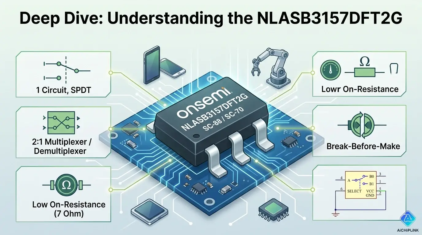
From the onsemi NLASB3157 datasheet — single-channel SPDT CMOS analog switch:
Switching function:
- Type: SPDT (Single-Pole Double-Throw) — one common (COM) terminal switches to either Y0 or Y1 based on the SEL control input
- Channels: 1 (one switch)
Key electrical parameters:
- RON (On-state resistance) typical: ~3Ω (mid-supply, room temperature)
- RON maximum: 4.5Ω at specified test conditions
- Supply voltage (VCC): 1.65V to 5.5V
- Signal voltage range: 0V to VCC (rail-to-rail analog signal capability)
- Propagation delay: 7.5 ns typical
- Bandwidth (−3 dB): >200 MHz (suitable for high-speed signal switching including LVDS)
Control (SEL pin):
- Logic levels track VCC (LVCMOS-compatible control)
- Overvoltage protection on control pin: voltages up to 7.0V above GND can be present on the SEL pin without damage, regardless of VCC level — allows a 5V logic controller to control an NLASB3157 running at 1.8V VCC without level-shifting
Temperature:
- Operating range: −55°C to +125°C — full industrial/automotive temperature range
Off-state isolation:
- Leakage current (off): < 1 nA at room temperature (extremely low — CMOS gate)
- Off-state capacitance: a few picofarads (signal integrity concern at high frequencies)
Package:
- SC-88 (SOT-363), 6 pins, 2mm × 2.1mm body
3.0 The Physics: How a CMOS Analog Switch Actually Works
Why a CMOS analog switch is not a mechanical relay:
A mechanical relay uses a physical contact that is either touching or not touching. When closed, the contact resistance is a few milliohms — essentially zero. The signal path is a metal-to-metal contact that is completely independent of the signal level. The signal does not affect the switch state, and the switch state does not distort the signal.
A CMOS analog switch uses a MOSFET transistor as the switching element. The transistor's channel (source-to-drain) is the signal path. The gate controls whether the channel is open or conducting. When the channel is conducting, its resistance (RON) is the resistance the signal experiences. But here is the critical difference from a relay: the MOSFET's RON depends on VGS (gate-to-source voltage), and VGS depends on the signal voltage being switched.
The transmission gate: complementary CMOS switch:
The NLASB3157 uses a CMOS transmission gate — a complementary pair of one NMOS and one PMOS transistor connected in parallel between COM and Y0/Y1. This complementary design is specifically chosen to reduce RON variation across the signal range:
- NMOS transistor: strong conduction when signal is near GND (VGS is large), weak conduction when signal is near VCC (VGS approaches zero)
- PMOS transistor: strong conduction when signal is near VCC (|VGS| is large), weak conduction when signal is near GND (|VGS| approaches zero)
The NMOS and PMOS contributions are complementary: where one weakens, the other strengthens. The parallel combination provides a more uniform total conductance across the signal range than either transistor alone.
RON vs signal voltage — the residual nonlinearity:
Even with the complementary transmission gate, RON is not perfectly constant across the signal range. The variation is specified in the datasheet as RON flatness (ΔR_ON) — typically a few ohms of variation across the full 0V to VCC signal range. This flatness characteristic determines the harmonic distortion of the switch for analog signals.
For a signal passing through a resistance that varies as a function of signal level, the output voltage is:
VOUT = VIN × RLOAD / (RON(VIN) + RLOAD)
Since RON(VIN) varies with VIN, the transfer function is nonlinear. This nonlinearity generates harmonic distortion — primarily second and third harmonics — proportional to the amplitude of RON variation. For the NLASB3157 with a few ohms of RON variation, driving into a high-impedance load (where RLOAD >> RON), the distortion is negligible. Driving into a low-impedance load (where RLOAD approaches RON), the distortion becomes significant.
4.0 Real Circuit Applications: When NLASB3157 Is the Right Switch
Application 1: Clock signal multiplexing (ideal application)
The NLASB3157 may be used for clock switching and data multiplexing, and can switch balanced signal pairs such as LVDS at >200 Mb/s. For clock switching, the signal is digital — it transitions rapidly between 0 and VCC with short dwell time at intermediate voltages. The nonlinearity of RON affects only the transition regions, not the steady-state levels. Clock switching is an ideal application: the RON nonlinearity causes negligible distortion on a digital signal, and the fast propagation delay (7.5 ns) enables switching high-frequency clocks.
Application 2: I/O bank switching and signal routing in mixed-voltage systems
The NLASB3157's supply range of 1.65V–5.5V covers all common CMOS logic voltages. Its control pin overvoltage tolerance (up to 7V) allows a 5V MCU to control an NLASB3157 operating at 1.8V VCC without a level shifter. This makes it useful for routing signals between different voltage-domain peripherals where both the signal and the control come from different supply domains.
Application 3: ADC input multiplexing with high-impedance sources
For multiplexing multiple sensor signals to a single ADC input, the NLASB3157 is appropriate when the signal source impedance is low (< 1 kΩ) and the ADC input impedance is high (> 10 kΩ). Under these conditions, the RON of 3–4.5Ω is negligible relative to the load impedance, and the nonlinearity creates distortion below the ADC's measurement resolution. For precision applications where 12-bit or 16-bit ADC accuracy must be maintained, verify that the RON variation does not cause gain error that exceeds the ADC's LSB size.
Application 4: Audio signal switching at line level
For switching audio signals (line level, 1V RMS, 10kΩ load), the NLASB3157 can work with very low audible distortion — its RON variation of a few ohms into a 10kΩ load produces a gain variation of ΔR_ON/RLOAD ≈ 0.03–0.05% — well below audible thresholds. However, for audiophile-grade applications with THD requirements below 0.001%, the charge injection at switching transients (described in Section 6) produces a click artifact that may be audible. For professional audio switching where both signal quality and switching transients matter, evaluate whether a reed relay or a specialty audio switch with matched charge injection cancellation better fits the requirement.
5.0 Five Misconceptions About CMOS Analog Switches
Misconception 1: "RON is a fixed value like a discrete resistor"
As explained above, RON varies with the signal voltage. The datasheet specifies RON at a single test condition (specific VCC, specific VIN, specific load) and a maximum value. The RON across the full signal range varies, and this variation is the source of analog distortion. For precision applications, check the RON vs VIN curve in the datasheet (usually Figure 1 or similar) to understand the actual variation at the operating conditions.
Misconception 2: "The switch works as a relay — signal can flow in either direction through COM freely"
A CMOS analog switch is bidirectional — signal current can flow from COM to Y0/Y1 or from Y0/Y1 to COM. However, the signal voltage must remain within the supply range (0V to VCC). If the signal voltage exceeds VCC or drops below GND, the internal protection diodes clamp the signal and the switch no longer functions as a linear pass element. Always verify that the signal amplitude range is within the supply range.
Misconception 3: "The off-state switch provides complete signal isolation"
The off-state CMOS switch has very low DC leakage (< 1 nA), which is excellent isolation for DC and low frequencies. But the off-state still has a parasitic capacitance (COFF, a few picofarads) between the signal terminals. At high frequencies, this capacitance provides a signal path: Z = 1/(2πfC). At 100 MHz with 3 pF off-state capacitance: Z = 530 Ω — significant signal feedthrough even with the switch "off." For RF or high-frequency signal isolation, the NLASB3157's off-state capacitance may allow unacceptable signal coupling.
Misconception 4: "Charge injection only matters in precision analog circuits"
Charge injection occurs when the switch transitions from on to off (or off to on) — the gate control signal couples charge through the gate-drain and gate-source capacitances into the signal path. This produces a voltage glitch on the signal output at the moment of switching. For high-speed digital signal routing, this glitch is a small perturbation below the switching threshold and is irrelevant. For precision analog circuits (ADC input switching between successive conversions, sample-and-hold circuits, audio switching), the charge injection glitch is a real source of error or audible artifact.
Misconception 5: "A lower RON is always better"
Lower RON reduces the signal attenuation through the switch (important when the load impedance is comparable to RON) and reduces thermal noise contributed by the switch resistance. But very low RON requires larger transistors, which have higher gate capacitance, which increases charge injection when switching. There is a design trade-off: the optimum RON depends on the application's priority between signal integrity during operation and transient behavior at switching events.
6.0 Design Notes: Charge Injection, Layout, and Overvoltage
Charge injection — understanding and minimizing:
When the SEL control pin transitions, the gate voltage change couples through CGSD (gate-source/drain overlap capacitance) into the signal path as a charge packet. The resulting voltage step on the output is:
ΔVOUT ≈ (CGSD × ΔVGATE) / (CLOAD + CGSD)
For a typical CMOS switch with CGSD ≈ 0.5 pF, ΔVGATE = VCC = 3.3V, and CLOAD = 10 pF: ΔVOUT ≈ (0.5 × 3.3) / (10 + 0.5) ≈ 157 mV — significant in a precision measurement context.
Minimization techniques:
- Increase CLOAD (add a bypass capacitor on the output) to reduce the fractional charge on the output: larger denominator in the above equation
- Slow the SEL transition: the NLASB3157 accepts logic-level SEL, so adding a small RC filter (1kΩ + 10pF) on the SEL pin slows the gate transition, distributing the charge injection over a longer time and reducing the peak glitch amplitude — at the cost of slower switching
- Use matched dummy switches: place an identical switch in the signal path with its SEL driven in phase, creating a matching charge injection that partially cancels
Control pin overvoltage:
The control pin has overvoltage protection that allows voltages above VCC up to 7.0V to be present on the SEL pin without damage or disruption of operation, regardless of the operating voltage. This is particularly useful in mixed-supply designs where the MCU operates at 5V but the switch runs at 1.8V — no level shifter required on the SEL line.
PCB layout for SC-88 (SOT-363) package:
The SC-88/SOT-363 is a 6-pin package with 0.65mm lead pitch on a 2mm × 2.1mm body. For signal integrity:
- Keep the COM, Y0, and Y1 signal traces short and direct
- Avoid routing the SEL control trace adjacent to signal traces — capacitive coupling from the digital control signal to the analog signal can cause crosstalk
- Place a 100nF bypass capacitor on VCC within 2mm of the package
- If switching differential signals (e.g., LVDS pairs), route complementary pair traces with matched length through the switch
7.0 Real Questions from Circuit Designers
Q: I am using NLASB3157DFT2G to multiplex two I²C buses to one controller. The switch occasionally causes I²C bus lockup after switching. What is happening?
A: I²C bus lockup after an analog switch transition is caused by the charge injection glitch on the SCL or SDA lines at the moment of switching. If the glitch occurs while the I²C controller is in the middle of a transaction, the controller and slave device may get out of synchronization — the slave sees a spurious clock edge or a noise pulse it interprets as a start/stop condition. Solutions: (1) only switch the I²C bus during idle periods (no active transactions on either bus); (2) after switching, issue a bus reset sequence before beginning communication; (3) add 100 pF capacitors on the SCL and SDA lines at the switch outputs to reduce the glitch amplitude. Many systems implement I²C bus switching with dedicated I²C multiplexer ICs (PCA9544, TCA9548) that handle bus isolation and glitch suppression more robustly than a general-purpose analog switch.
Q: Can NLASB3157DFT2G switch RF signals at 433 MHz for a short-range wireless design?
A: At 433 MHz, the NLASB3157's off-state capacitance (COFF ≈ 2–3 pF) presents approximately 120–180 Ω of impedance in the off state — providing limited isolation at RF frequencies. The on-state insertion loss from RON = 3Ω into a 50Ω RF system is approximately 20×log10(50/(50+3)) ≈ 0.5 dB per switch — acceptable but not ideal. For occasional RF switching at 433 MHz with relaxed insertion loss and isolation requirements, the NLASB3157 can function, but dedicated RF switches (PE42422, MACOM MASWSS0180, or similar GaAs or SiGe SPDT RF switches) provide dramatically better insertion loss (< 0.3 dB) and off-state isolation (> 30 dB) specifically designed for RF signal path use. For 433 MHz RF, use an RF switch; for IF or baseband analog signal routing, the NLASB3157 is appropriate.
Q: The NC7SB3157 is specified on our existing PCB. Is NLASB3157DFT2G a direct replacement?
A: Yes — the NLASB3157DFT2G is specifically designed as a drop-in replacement for the NC7SB3157. It is pin-compatible (same SC-88/SOT-363 package, same pinout) and electrically equivalent or improved (similar or better RON, same supply range, same control interface). No PCB changes are required. The NLASB3157 may have slightly different RON at some operating corners compared to NC7SB3157 — verify against the specific test conditions in your application if precision matching is required — but for standard digital signal switching and general analog routing applications, the substitution is direct and transparent.
8.0 Quick Reference Card
Part Number Decode:
| Field | Value | Meaning |
|---|---|---|
| NLA | NLA | onsemi Next-Level Analog family |
| SB | SB | Small Bus / Signal switch |
| 3157 | 3157 | SPDT, ~3Ω RON product family |
| D | D | SC-88 (SOT-363) package |
| F | F | Package lead variant |
| T2 | T2 | Tape-and-reel, 3,000/reel |
| G | G | RoHS compliant, lead-free |
Key Specifications:
| Parameter | Value |
|---|---|
| Function | SPDT (1 common → 2 outputs) |
| RON typical | ~3Ω |
| RON maximum | 4.5Ω |
| VCC range | 1.65V to 5.5V |
| Signal range | 0V to VCC (rail-to-rail) |
| Propagation delay | 7.5 ns |
| SEL overvoltage | Up to 7V (safe above VCC) |
| Temperature | −55°C to +125°C |
| Package | SC-88 (SOT-363), 6 pins, 2×2.1mm |
Why RON ≠ Fixed Resistor:
RON varies with signal voltage because MOSFET VGS changes as the signal changes. The complementary NMOS+PMOS transmission gate flattens RON across the range — but ΔR_ON remains, causing:
- Low-impedance loads: signal attenuation varies → harmonic distortion
- High-impedance loads: attenuation negligible → distortion negligible
The Three Key Design Rules:
- Signal range: Keep signal within 0V to VCC — outside this range, protection diodes clamp
- SEL timing: Switch only during signal-inactive periods to avoid glitch propagation
- High-frequency isolation: COFF (≈ 2–3 pF) limits off-state isolation above ~100 MHz
NC7SB3157 compatibility: Direct drop-in replacement — same package, same pinout, same function.
For sourcing onsemi NLASB3157DFT2G with verified authenticity and competitive pricing, visit aichiplink.com.

Written by Jack Elliott from AIChipLink.
AIChipLink, one of the fastest-growing global independent electronic components distributors in the world, offers millions of products from thousands of manufacturers, and many of our in-stock parts is available to ship same day.
We mainly source and distribute integrated circuit (IC) products of brands such as Broadcom, Microchip, Texas Instruments, Infineon, NXP, Analog Devices, Qualcomm, Intel, etc., which are widely used in communication & network, telecom, industrial control, new energy and automotive electronics.
Empowered by AI, Linked to the Future. Get started on AIChipLink and submit your RFQ online today!
Frequently Asked Questions
What is NLASB3157DFT2G used for?
The NLASB3157DFT2G is a compact SPDT CMOS analog switch used for routing low-voltage analog or digital signals in applications like clock multiplexing, ADC input selection, audio signal switching, and mixed-voltage signal path control. Its low 3Ω typical RON, fast 7.5 ns switching, and 1.65V–5.5V operating range make it ideal for embedded systems and signal multiplexing designs.
Why is RON not a fixed resistance?
Unlike a resistor, the on-resistance of NLASB3157DFT2G changes with signal voltage because it is formed by CMOS transmission-gate MOSFET channels whose conductivity depends on gate-to-source voltage. This varying RON can introduce small nonlinear distortion in precision analog applications, especially when driving lower-impedance loads.
Is NLASB3157DFT2G a replacement for NC7SB3157?
Yes. NLASB3157DFT2G is a direct drop-in replacement for NC7SB3157, offering pin compatibility, equivalent electrical performance, and the same SC-88/SOT-363 footprint, making migration easy for legacy Fairchild-based designs.
Can it handle high-speed or RF signals?
The device supports bandwidth above 200 MHz, making it suitable for fast digital clocks, LVDS routing, and general signal multiplexing, but its parasitic capacitance and limited RF isolation make it less suitable for dedicated RF switching applications like 433 MHz wireless front ends, where specialized RF switch ICs perform better.
What are the main design precautions?
When using NLASB3157DFT2G, keep signals within 0V to VCC, minimize PCB trace length, place decoupling capacitors close to the package, avoid switching during active signal transitions to reduce charge-injection glitches, and account for off-state capacitance if high-frequency isolation is important.


.png&w=256&q=75)


