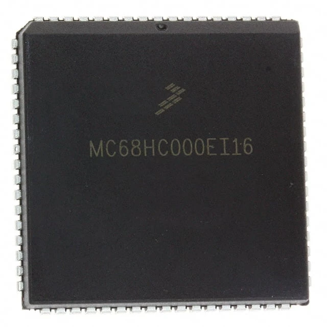
Here is a situation more common than most engineers admit: you are maintaining a production automotive ECU designed in the mid-1990s. The board uses an MC68HC11F1 in a 68-pin PLCC package. The original engineer retired. The firmware is in a .s19 file on a floppy disk image someone recovered from an old PC. The customer needs 500 more units, and the MCU in question is the MCHC11F1CFNE4 — NXP's (formerly Freescale, formerly Motorola) 8-bit HC11 microcontroller, still in limited production, still listed on Aichiplink.
If that scenario sounds familiar, this guide is written specifically for you. If you are evaluating the HC11 for a genuinely new design — stop. There are better choices in 2025, and this article will tell you exactly what to use instead. But if you are maintaining, repairing, or procuring parts for a legacy HC11 system, read on: the MCHC11F1CFNE4 has more nuance than any distributor listing will show you, and getting the wrong variant has derailed more than one maintenance project.
1.0 What Exactly Is the MCHC11F1CFNE4?
The part number encodes everything you need to know — if you know how to read it.
MC — Motorola/Freescale/NXP product prefix
HC11 — 68HC11 8-bit CISC microcontroller family
F1 — F1 variant: ROMless (no internal program ROM), 1KB RAM, 512B EEPROM, expanded bus capable
C — Operating temperature: C = Commercial/Automotive (−40°C to +85°C)
F — Package: F = PLCC (Plastic Leaded Chip Carrier)
N — 68-pin package
E — Package material/process indicator
4 — Tape and reel / packaging format (4 = tube/tray in this context)
The critical letter in this part number is F1 — this is the ROMless variant of the HC11 family. It has no internal program ROM. This means the MCU cannot run standalone from internal memory in normal single-chip mode. It requires either:
- An external memory bus with external program ROM/EPROM (expanded mode), or
- Bootstrap mode via SCI to download code into the 1KB internal RAM
This is the most common source of confusion when engineers who are familiar with other HC11 variants (like the HC11E9 with 12KB ROM, or the HC11A8 with 8KB ROM) try to bring up a MCHC11F1CFNE4 board for the first time and watch it do absolutely nothing.
Compare within the HC11F1 ordering family:
| Part Number | Temp Grade | Package | Pins | Notes |
|---|---|---|---|---|
| MCHC11F1CFNE4 | −40°C to +85°C | PLCC | 68 | Automotive; tube packaging |
| MCHC11F1VFNE3 | −40°C to +85°C | PLCC | 68 | 3.3V/5V compatible variant |
| MCHC11F1CFNE3R | −40°C to +85°C | PLCC | 68 | Tape-and-reel (R suffix) |
| MC68HC11F1CFN2 | −40°C to +85°C | PLCC | 68 | Older Motorola part number |
Pro Tip: The MCHC11F1CFNE4 and the older MC68HC11F1CFN2 are electrically identical. If you are cross-referencing legacy BOMs, these two part numbers refer to the same silicon with a rebranding during the Motorola → Freescale → NXP transition.
2.0 Full Specifications: What You Actually Get
The MCHC11F1CFNE4 is an 8-bit MCU with 1KB RAM and 512B EEPROM, operating at 4 MHz from a 4.75V to 5.25V supply, with 54 I/O pins in a 68-pin PLCC package, operating from −40°C to +85°C.
Here is the complete parameter set:
- CPU Architecture: M68HC11 CISC, 8-bit accumulator (A, B registers; 16-bit D = A:B)
- CPU Clock: 4 MHz (E-clock = 2 MHz; most instructions execute in 2–5 E-cycles)
- Internal ROM: None — ROMless (the defining characteristic of F1)
- Internal RAM: 1,024 bytes (1 KB), battery-backed with appropriate external circuit
- EEPROM: 512 bytes, 10,000 P/E cycle endurance, 10ms erase/program time
- External Bus: Full 16-bit address + 8-bit data multiplexed bus, supports up to 64 KB external memory
- I/O Ports: Up to 54 GPIO pins depending on operating mode and peripheral configuration
- ADC: 8-channel, 8-bit successive approximation ADC (PORTA, pins PA0–PA7); requires VRH/VRL reference pins
- Timers: One 16-bit free-running timer with 4 input captures, 5 output compares, overflow interrupt
- Serial Communications Interface (SCI): Full-duplex UART, configurable baud rate from E-clock
- Serial Peripheral Interface (SPI): Synchronous master/slave serial, configurable clock phase/polarity
- Chip Selects: 8 hardware chip select signals (STRA, STRB, PE3–PE6 configurable) for external memory/peripheral mapping
- STOP/WAIT power modes: Reduced power states; STOP mode draws < 500 µA
- Supply Voltage: 4.75 V to 5.25 V (5V nominal; not 3.3V tolerant)
- Operating Temperature: −40°C to +85°C
- Package: 68-pin PLCC (24.21 mm × 24.21 mm, 1.27 mm lead pitch)
- ESD Rating: 2 kV HBM per JEDEC
What it does NOT have (common misconception items):
- No internal program ROM — cannot boot from internal flash or ROM
- No hardware multiply/divide — integer math is software-emulated
- No DMA controller
- No CAN bus peripheral (HC11 predates automotive CAN adoption)
- No 3.3V operation — strictly 5V only
3.0 Operating Modes — The Decision That Defines Your Firmware
The HC11F1 supports four operating modes selected by the MODA and MODB pin states at reset. For the ROMless F1 variant, only two modes are practically useful:
Expanded Multiplexed Mode (MODA=1, MODB=1):
The MCU uses PORT B (8-bit data bus), PORT C (8-bit address, lower byte), and PORT B (address upper byte via STRA strobe) to implement a full external 16-bit address space. This is the required mode for nearly all MCHC11F1CFNE4 designs — the MCU fetches its reset vector and program code from external EPROM/EEPROM mapped at address $FFFE/$FFFF and up.
The external memory map in expanded mode provides 64KB addressable space, though the internal RAM ($0000–$00FF default) and EEPROM ($B600–$B7FF default) remain present. Eight chip select outputs (configurable via the INIT, HPRIO, and CONFIG registers) allow hardware-decoded address ranges for external peripherals.
Bootstrap Mode (MODA=0, MODB=0):
A special factory-programmed bootstrap ROM ($BFC0–$BFFF) appears in the memory map. At power-up, the bootstrap ROM initializes the SCI at a fixed baud rate (determined by crystal frequency), then waits to receive 256 bytes via the SCI RXD pin. Those 256 bytes are loaded into internal RAM starting at $0000 and executed.
Bootstrap mode is how you:
- Program the CONFIG EEPROM register (which controls boot mode and COP watchdog)
- Download and run diagnostic firmware
- Recover a board where the CONFIG register has been set to an unusable mode
Single-Chip Mode (MODA=0, MODB=1):
Disables the external bus and makes all PORT B and PORT C pins available as GPIO. Useless for the F1 variant since there is no internal ROM to execute from. Avoid.
Special Test Mode (MODA=1, MODB=0):
Freescale factory use only. Do not use in production.
⚠️ Critical Warning: The CONFIG register in EEPROM controls whether the external bus is enabled after reset. If a previous firmware accidentally cleared the EXTR bit in CONFIG, the MCU will start in single-chip mode even with MODA/MODB pulled high — appearing completely dead on the external bus. Recovery requires bootstrap mode via SCI.
4.0 On-Chip Peripherals: Timer, SCI, SPI, ADC
16-Bit Timer System:
The HC11's timer is one of its most capable features. The free-running 16-bit counter (TCNT) clocks at E/4 (500 kHz at 4MHz crystal). Five Output Compare registers (OC1–OC5) allow hardware-timed PWM generation and event scheduling without CPU intervention. Four Input Capture registers (IC1–IC4) timestamp external events to 2 µs resolution. Timer Overflow interrupt occurs every 131 ms at 4 MHz — critical to account for in time-keeping firmware.
SCI (Serial Communications Interface):
Standard full-duplex UART. Baud rate = E-clock / (16 × BAUD_divider). At 4 MHz, common achievable baud rates include 1200, 2400, 4800, 9600, 19200 bps. The SCI uses TXD (PD1) and RXD (PD0). Note: there is no hardware FIFO — received characters must be read before the next character arrives (at 9600 baud, you have ~1 ms). Missing characters due to CPU interrupt latency is a common bug in HC11 firmware.
SPI (Serial Peripheral Interface):
Synchronous 8-bit master or slave. CPOL and CPHA bits configure clock polarity and phase for any SPI mode (0, 1, 2, 3). SCK available up to E/2 (1 MHz at 4 MHz crystal) in master mode. Uses PD2 (MISO), PD3 (MOSI), PD4 (SCK), PD5 (SS). Note: the HC11 SPI does not automatically assert SS — firmware must manually control the SS pin.
8-bit ADC:
Eight multiplexed analog input channels (PORTA, PA0–PA7). Result register (ADR1–ADR4) holds last four conversions after a single conversion or continuous scan. Reference voltage pins VRH and VRL must be properly decoupled — VRH connected to 5V through a 1 µF + 100 nF filter is mandatory; failure to do this is the single most common cause of noisy ADC readings on HC11 boards.
5.0 ⚠️ Five Pitfalls Engineers Hit with the HC11F1 (And How to Avoid Them)
These are real failure modes, not textbook warnings. Each one has caused production delays.
Pitfall 1: CONFIG Register Lock-Out
The CONFIG register lives in EEPROM and is read at reset to configure operating mode, COP watchdog, and NOCOP bit. If your firmware writes an incorrect value to CONFIG (or fails to disable the COP watchdog with NOCOP=1 during development), the MCU will reset continuously or boot into the wrong mode. Recovery: bootstrap mode via SCI at the correct baud rate. Prevention: always make CONFIG register programming the last step of firmware bring-up, and verify with a SCI terminal before releasing to production.
Pitfall 2: Voltage at XIRQ or IRQ Pins Before VDD Stabilizes
During power-on, if XIRQ or IRQ pins receive a valid assertion before VDD fully stabilizes, the HC11 can vector to an interrupt handler before the stack pointer is initialized — corrupting whatever memory the stack lands in and producing bizarre startup behavior. Solution: add 10 kΩ pull-up resistors on XIRQ and IRQ lines, and ensure external devices driving these pins have power-on reset delays.
Pitfall 3: External Bus Timing Violations at PCB Trace Lengths Above 10 cm
The HC11's external bus runs at 2 MHz (one E-clock = 500 ns). This sounds slow, but address setup time (tAS) and data setup time (tDS) are tighter than many engineers expect on the timing diagram. PCB trace lengths above 10 cm introduce enough propagation delay and capacitive loading to violate these margins with standard 74HC-series memory. Solution: verify with an oscilloscope that AS (Address Strobe) and E-clock edges have clean transitions at the external memory device pins. Add series resistors (33–47 Ω) on address and data bus lines to damp reflections.
Pitfall 4: ADC Inaccuracy from Shared VDD Reference
Connecting VRH directly to VDD without filtering is the most common HC11 ADC mistake. The MCU's own switching activity couples noise onto VDD, which then directly contaminates the ADC reference voltage. Every output port switching produces a measurable glitch on VRH. Fix: filter VRH separately — route a 10 Ω resistor from VDD to VRH, then decouple with 10 µF + 100 nF to AGND. Keep AGND separated from DGND and join at a single star point near the power supply.
Pitfall 5: Confusing MCHC11F1CFNE4 with HC11E-series Parts
The HC11E9 has 12KB internal ROM, 512B EEPROM, 512B RAM — and boots in single-chip mode. The MCHC11F1CFNE4 has zero internal ROM, requires external memory, and will appear completely dead if you pull MODA/MODB incorrectly. Engineers who have only used E-series HC11s and then receive F1 parts for a maintenance job invariably spend an afternoon convinced the parts are defective. They are not. The F1 requires an external memory bus.
6.0 Modern Substitutes: When to Replace the HC11 and What to Use
If you are starting a new design in 2025, the HC11 is not the right choice. Here is an honest comparison with modern alternatives:
| Parameter | MCHC11F1CFNE4 (HC11) | NXP S08 / S12 Family | Microchip PIC18 Series | STM32G0 Series |
|---|---|---|---|---|
| Architecture | 8-bit CISC | 8/16-bit | 8-bit RISC | 32-bit ARM Cortex-M0+ |
| Max Clock | 4 MHz | 8–40 MHz | 64 MHz | 64 MHz |
| Flash | None (external) | 4 KB – 256 KB internal | 2 KB – 128 KB internal | 16 KB – 512 KB internal |
| RAM | 1 KB | 256B – 16 KB | 256B – 8 KB | 4 KB – 144 KB |
| Supply Voltage | 5V only | 1.8V – 5.5V | 1.8V – 5.5V | 1.7V – 3.6V |
| Package options | PLCC-68 only | QFP, QFN, DIP | DIP, QFP, QFN | QFP, QFN, UFQFPN |
| Development tools | Legacy CodeWarrior | Free MCUXpresso | Free MPLAB X | Free STM32CubeIDE |
| In production | Limited (end-of-life risk) | Active | Active | Active |
When to keep the HC11:
You are maintaining an existing certified product (medical, automotive) where re-certification after an MCU change is prohibitively expensive. The board is already designed and tooled. The firmware source code is lost and you are running binary-only. Replacement is not cost-justified for the production run size.
When to replace with a modern MCU:
Any new design. Any existing design where the firmware source is available and the production volume justifies one-time re-engineering cost.
Best modern pin-count-compatible substitute: The NXP S08 family (MC9S08AC128) shares Freescale heritage, similar programmer tools, and automotive qualification. Migration requires porting firmware but the peripheral model is similar enough that an experienced engineer can complete a basic port in days. For a clean-sheet replacement, the STM32G031 (32-bit, 64 MHz, −40°C to +85°C, LQFP-32 or TSSOP-20) offers 16× the clock speed, 256× the flash, and 64× the RAM at a lower unit cost.
7.0 PCB and Hardware Design Notes for PLCC-68
The PLCC-68 is a through-hole-compatible surface-mount package with J-bend leads on 1.27 mm pitch. Key layout notes:
Power decoupling is mandatory and specific. The HC11 requires:
- One 10 µF tantalum capacitor per VDD pin, placed within 10 mm
- One 100 nF X7R ceramic capacitor per VDD pin, placed within 5 mm
- Separate filter network for VRH as described in Section 5 (Pitfall 4)
- AGND and DGND separated and joined at a single point
Crystal / clock oscillator:
The EXTAL/XTAL pins accept either a crystal (with 22 pF load capacitors to GND) or a TTL-level clock input on EXTAL with XTAL left floating. At 4 MHz crystal, the internal E-clock runs at 2 MHz (E = crystal/2). Use AT-cut crystals with load capacitance specified to match the crystal's datasheet; wrong load capacitance causes oscillator startup failure — another common bring-up problem.
PLCC socket for development:
During development and for boards that require field replacement, use a machined PLCC-68 socket (e.g., Yamaichi IC51-0682-808). PLCC sockets are available in both SMD and through-hole versions. Through-hole PLCC sockets allow easy removal/replacement without hot-air rework tools.
MODA / MODB strapping:
Pull MODA and MODB high (to VDD through 10 kΩ resistors) for expanded mode. These pins must be stable before RESET deasserts — place the pull-up resistors within 15 mm of the MCU.
RESET pin:
Use a dedicated supervisory reset IC (e.g., Maxim MAX809, Texas Instruments TPS3836) for reliable power-on reset. The internal power-on reset circuit of the HC11 has marginal noise immunity — relying on it alone causes erratic behavior during slow power ramp-ups (common with large bulk capacitors).
8.0 Quick Reference Card
Operating Mode Selection:
| MODA | MODB | Mode | Use for F1? |
|---|---|---|---|
| 0 | 0 | Bootstrap | Yes — for CONFIG programming and recovery |
| 0 | 1 | Single-Chip | No — no internal ROM |
| 1 | 0 | Special Test | No — factory only |
| 1 | 1 | Expanded Multiplexed | Yes — primary mode for all F1 designs |
CONFIG Register Key Bits (EEPROM address $103F):
| Bit | Name | Function |
|---|---|---|
| 3 | NOSEC | Security disable (set to 1 normally) |
| 2 | NOCOP | COP watchdog disable (set to 1 during development) |
| 1 | ROMON | ROM enable (always 0 for F1 — no ROM) |
| 0 | EEON | EEPROM enable in memory map |
Minimum External Components for Expanded Mode:
- 4 MHz crystal + 2× 22 pF load capacitors
- 10 kΩ pull-ups on MODA, MODB
- Supervisory reset IC (MAX809 or equivalent)
- 10 µF + 100 nF decoupling per VDD pin
- 10 Ω + 10 µF + 100 nF filter on VRH (for ADC)
- External 32 KB EPROM (27C256 or equivalent) mapped to $8000–$FFFF
For sourcing the MCHC11F1CFNE4 or compatible HC11 family parts, visit aichiplink.com for verified inventory and competitive pricing.

Written by Jack Elliott from AIChipLink.
AIChipLink, one of the fastest-growing global independent electronic components distributors in the world, offers millions of products from thousands of manufacturers, and many of our in-stock parts is available to ship same day.
We mainly source and distribute integrated circuit (IC) products of brands such as Broadcom, Microchip, Texas Instruments, Infineon, NXP, Analog Devices, Qualcomm, Intel, etc., which are widely used in communication & network, telecom, industrial control, new energy and automotive electronics.
Empowered by AI, Linked to the Future. Get started on AIChipLink.com and submit your RFQ online today!
Frequently Asked Questions
Why is my HC11F1 board completely unresponsive after power-on?
Most likely a mode configuration issue. Ensure MODA and MODB are HIGH at reset (expanded mode). If still no activity, enter bootstrap mode and check the CONFIG register—make sure EXTR = 1 (external bus enabled).
Can I replace MCHC11F1CFNE4 with MCHC11F1VFNE3?
Technically yes in a 5V system, but for automotive ECUs, any component change usually requires re-certification or formal approval. Do not substitute without validation.
Is EEPROM failure after a few years normal?
Yes. HC11 EEPROM is rated for 10,000 write cycles and ~10 years at 25°C. At high temperatures (e.g., 85°C), retention may drop to 3–5 years. Reduce write frequency or use RAM for frequently updated data.
Can I run a program using only the 512B EEPROM?
Theoretically yes, but highly impractical. The space allows only very small programs (tens of instructions). Most real applications require external memory.
Are there still development tools available for HC11?
Yes. Common options include: VASM (recommended, cross-platform) GCC (older M6811 versions) CodeWarrior (runs in compatibility mode) AS11 assembler


