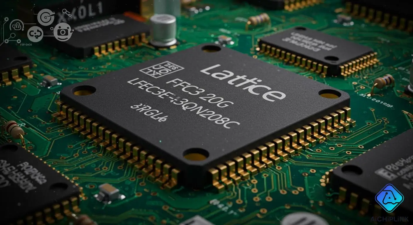
You will see that the lattice lfec3e-3qn208c is a cheap fpga from Lattice Semiconductor. This chip has a 208-pin QFP package. It supports over 140 I/O pins. It has 3.1K LUTs. You can use it up to 340MHz speed. The core voltage is 1.2V. It uses 130nm technology. Many designers pick the lfec3e-3qn208c fpga because it uses little power. It also has balanced resources.
Here is how it matches up with other common FPGAs:
| Advantages | Disadvantages |
|---|---|
| Cheap FPGA for designs that need to save money | Lower top speed than fancy FPGAs |
| Uses less power than many other choices | Not much logic space and memory |
| Balanced resources without too much extra | Might become outdated since it is an older model |
| Good support and works well for many years | Does not have special features like DSP blocks |
| Can be set up with JTAG or sysCONFIG modes | Must balance power and speed at high use |
Key Takeaways
-
The Lattice LFEC3E-3QN208C FPGA is a good choice if you want to save money. It works well for projects that need lots of I/O connections and use little power.
-
This FPGA can run at speeds up to 340MHz. It has 145 I/O pins. This makes it good for many digital projects.
-
You can use programming tools like Lattice Diamond or ispLEVER. These tools help you design and put your logic into the FPGA easily.
-
Always look at the datasheet for more details and pin layouts. This will help your project work well.
-
If you need more logic or faster speeds, look at other Lattice EC family options.
Lattice LFEC3E-3QN208C Features
Main Features
The lattice lfec3e-3qn208c has many helpful features. It comes in a 208-pin QFP package. There are more than 140 i/o pins for connecting devices. You can use about 3,100 logic elements to build circuits. The core voltage is 1.2V. The i/o banks work with voltages from 1.2V to 3.3V. This fpga can run at speeds up to 340MHz. It uses 130nm technology, which helps save power. The chip has on-chip memory and programmable i/o cells. It supports many i/o standards. The modular banked design lets you use mixed-voltage systems easily.
Tip: You can program the lattice lfec3e-3qn208c with JTAG or sysCONFIG. This makes setup and testing easier.
Specifications Table
You should look at the specifications before you start your project. The table below lists the main specifications for the lfec3e-3qn208c fpga.
| Feature | Specification / Description |
|---|---|
| Package Type | 208-pin QFP |
| I/O Count | 145 |
| Logic Capacity | About 3,100 logic elements |
| On-chip Memory | 56,320 bits of block RAM and distributed RAM |
| Operating Voltage | Core: 1.2V; I/O banks: 1.2V to 3.3V |
| Maximum Frequency | Up to 340MHz |
| Technology | 130nm CMOS |
| Memory Interface Support | DDR SDRAM up to DDR-400 (200 MHz clock) |
| I/O Standards | LVCMOS, LVTTL, SSTL, HSTL, PCI, LVDS |
| In-system Programmability | JTAG and sysCONFIG |
| Debugging Capabilities | ispTRACY logic analyzer support |
| Family | LatticeEC |
Block and Bank Diagram
You can learn about the inside of the lattice lfec3e-3qn208c by looking at its block and bank diagrams. These diagrams show how the fpga arranges its features and i/o resources.
-
The block diagram shows programmable i/o cells for device connections.
-
You can see programmable units for making custom logic.
-
Embedded block RAMs give fast memory for storing data.
-
System resources like sysCLOCK PLLs help with clock control.
-
The sysCONFIG and JTAG ports make programming and testing simple.
Note: If you want to use this fpga, check the block and bank diagrams in the datasheet. These pictures help you plan your i/o and logic layout.
LFEC3E-3QN208C FPGA Applications
Typical Uses
The lfec3e-3qn208c fpga is used in many digital projects. It is a good choice when you need to connect many devices. The high i/o count lets you link things like sensors or screens. You can make custom logic circuits that move data fast. Many engineers use this fpga for jobs that need steady work but not the fastest speed.
Here are some ways people use this fpga:
-
Make control units for robots or machines.
-
Build boards that process data for test tools.
-
Design special communication links with the flexible i/o.
-
Create signal converters for systems with different voltages.
-
Use the on-chip memory for small data storage or lookup tables.
Tip: The lattice lfec3e-3qn208c gives you a good mix of power and speed. Its i/o banks can work with many voltage levels.
Industry Examples
The lfec3e-3qn208c fpga is found in many fields. Companies use this fpga in products that need strong digital control and flexible i/o. Here are some real-life examples:
-
Industrial Automation: This fpga is used in motor controllers, PLCs, or factory sensors. The high i/o count helps connect to many devices at once.
-
Test and Measurement: Engineers use this fpga in oscilloscopes, logic analyzers, or signal generators. Fast speed and on-chip memory help process signals quickly.
-
Communications: This fpga is found in network switches or protocol converters. The flexible i/o standards help match different communication needs.
-
Consumer Electronics: Some audio or video devices use this fpga for custom signal paths or changing data.
Note: The lfec3e-3qn208c fpga works well for mid-range designs. You can trust its i/o features to handle tough connections in your project.
Alternatives and Comparison
Similar FPGAs
If you want a different FPGA, there are other choices in the Lattice EC family. The LFEC3E-3TN144C is very close to the LFEC3E-3QN208C. You can also look at the LFEC6E-3QN208C or LFEC1E-3T100C. These chips have different amounts of logic and i/o. Some chips have more logic elements or more i/o pins. Others can run faster for high-speed designs.
Think about what your project needs most. If you need more i/o pins, pick a chip with a higher i/o count. If you want more logic, choose one with more logic density. Some of these chips cost more money. But they give you better features or faster speeds. You can use these for bigger or faster projects.
Note: Always read the datasheet for each FPGA. This helps you find the best chip for your project.
Comparison Table
The table below shows how the LFEC3E-3QN208C compares to other options. You can see the main differences in price, speed, logic, and i/o.
| Attribute | Lattice LFEC3E-3QN208C | Alternatives |
|---|---|---|
| Cost | Low | Higher |
| Performance | Lower ceiling | Higher |
| Logic Density | Limited | Higher |
| I/O Count | Moderate | Varies |
| Core Voltage Range | Compatible with various | Varies |
The LFEC3E-3QN208C is a good choice if you want to save money. It works well for projects that do not need the fastest speed or most logic. The i/o count is enough for many uses. But some other chips have even more i/o pins. If you need more speed or logic, you can pick another FPGA from the same family. Each chip has its own mix of price, i/o, and speed.
Tip: Always check what your project needs for i/o and speed before you pick a chip. Choosing the right FPGA can help you save time and money.
Programming and Packaging
Programming Steps
You can program the LFEC3E-3QN208C fpga using simple tools. Start by choosing a design tool like Lattice Diamond or ispLEVER. These tools help you create your logic design. After you finish your design, you can use the JTAG or sysCONFIG port to load your program into the fpga. JTAG is a common way to test and update your design. You connect your computer to the fpga board with a cable. The software sends your program to the chip. You can also use sysCONFIG for in-system programming. This method lets you update the fpga while it stays on your board.
Tip: Always check your i/o settings before you program the fpga. This helps you avoid errors and protects your board.
Pros and Cons
You will find that the LFEC3E-3QN208C fpga has both strengths and weaknesses. Here is a quick list to help you decide if it fits your project:
Pros:
-
You get a high i/o count for connecting many devices.
-
The fpga uses low power, which helps with energy savings.
-
You can use standard tools for programming and debugging.
-
The chip gives stable performance for most mid-range tasks.
Cons:
-
The fpga does not have advanced features like DSP blocks.
-
You may find limited logic space for very large designs.
-
The performance may not match newer or high-end fpgas.
Package Details
The LFEC3E-3QN208C fpga comes in a 208-pin QFP package. QFP stands for Quad Flat Package. This type of package has pins on all four sides. The 208-pin QFP measures about 28 mm x 28 mm. The i/o pins are easy to solder to a printed circuit board. You can use this package in many types of projects. The large number of i/o pins lets you connect to many sensors, displays, or other chips. The package also helps with heat control, which keeps your fpga running well.
Note: Always check the datasheet for the exact pin layout and i/o bank locations. This helps you plan your board and get the best performance.
Datasheet and Resources
Datasheet Access
You need the correct datasheet before using the LFEC3E-3QN208C fpga. The datasheet has all the technical facts, pin maps, and voltage limits. You can get the official datasheet from the Lattice Semiconductor website. This file helps you plan your circuit and avoid errors. Many engineers use the datasheet to check voltage and timing details.
If you want to buy this fpga, use trusted sellers. The table below shows a good place to order the chip and get fast shipping.
| Distributor | Product | Availability | Link |
|---|---|---|---|
| EIS Components | LFEC3E-3QN208C | IN STOCK, ships within 24 hours | EIS Components Product Page |
Tip: Always get the newest datasheet before you design your board. This keeps your fpga project safe and current.
Manufacturer Info
Lattice Semiconductor makes the LFEC3E-3QN208C fpga. You can trust this company because it has been around for a long time. Lattice started in 1983 and went public in 1989. The company is in Hillsboro, Oregon, in the Silicon Forest. Over 1,000 people work for Lattice worldwide.
-
Lattice works on low power fpga solutions.
-
The company is known for new ideas in communications, computing, and cars.
-
In 2022, Lattice became the last big independent fpga maker after AMD bought Xilinx.
You can count on Lattice for good support and quality products. If you need more help, the company website has extra guides, notes, and the newest datasheet for every fpga model.
You now know the LFEC3E-3QN208C offers a strong mix of high I/O count, low power use, and steady performance. You can use this fpga in control systems, test tools, or communication devices. When you compare it to other chips, you see it gives good value for many projects. Always review the datasheet for details. If you plan to design with this chip, start by testing simple circuits and explore more features as you learn.

Written by Jack Elliott from AIChipLink.
AIChipLink, one of the fastest-growing global independent electronic components distributors in the world, offers millions of products from thousands of manufacturers, and many of our in-stock parts is available to ship same day.
We mainly source and distribute integrated circuit (IC) products of brands such as Broadcom, Microchip, Texas Instruments, Infineon, NXP, Analog Devices, Qualcomm, Intel, etc., which are widely used in communication & network, telecom, industrial control, new energy and automotive electronics.
Empowered by AI, Linked to the Future. Get started on AIChipLink.com and submit your RFQ online today!
Frequently Asked Questions
What tools can you use to program the LFEC3E-3QN208C FPGA?
You can use Lattice Diamond or ispLEVER software. These tools help you design and load your logic into the FPGA. JTAG and sysCONFIG ports let you program and test your chip.
How many I/O pins does the LFEC3E-3QN208C have?
You get 145 I/O pins with this FPGA. These pins let you connect sensors, displays, or other chips. The high I/O count makes it easy to build complex projects.
Can you use the LFEC3E-3QN208C for high-speed designs?
You can run this FPGA up to 340MHz. This speed works for many control and data tasks. If you need more speed, you should look at newer or higher-end FPGAs.
What package type does the LFEC3E-3QN208C use?
The LFEC3E-3QN208C comes in a 208-pin QFP package. QFP stands for Quad Flat Package. You can solder it easily to most circuit boards.