K4A4G165WF-BITD: The "95°C" Temperature Rating That Is Not What You Think It Is
When a datasheet says a DDR4 chip is rated to 95°C, most engineers read that as a maximum junction temperature — the temperature of the silicon die itself. For most semiconductors, that is exactly what it means. For the K4A4G165WF-BITD, and for virtually all commercial and industrial DRAM devices, the temperature specification is TC: case temperature, not TJ: junction temperature.
The distinction matters more than it sounds. Case temperature is measured at the top surface of the package. Junction temperature — the actual temperature inside the silicon — is always higher than case temperature by an amount determined by the device's power dissipation and the thermal resistance from junction to case (θJC). A DDR4 chip consuming 500 mW with a θJC of 5°C/W has a junction temperature 2.5°C above its case temperature. At moderate power levels, the TC/TJ gap in DRAM is relatively small compared to, say, a power MOSFET. But it is not zero, and a design that treats the 95°C TC rating as a junction temperature maximum will be operating the silicon at slightly elevated temperature relative to its qualified range.
The second thing the "BITD" suffix encodes that engineers often overlook: the I identifies this as the industrial temperature variant (−40°C to +95°C TC), distinguishing it from the commercial-grade "BCTD" sibling (0°C to +95°C TC). For embedded industrial hardware deployed outdoors, in vehicle cabinets, or in unheated enclosures, the cold-side guarantee is as important as the hot-side limit. A commercial-grade DRAM part is not characterized below 0°C — its timing and initialization behavior at −25°C ambient are not guaranteed. The BITD's −40°C rating provides that guarantee.
These two points — TC vs TJ semantics, and the cold-side industrial guarantee — are what the K4A4G165WF-BITD is specifically about.
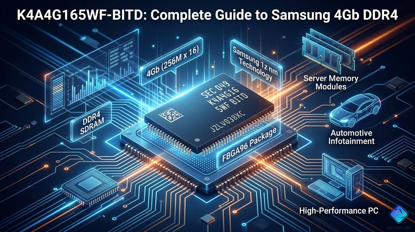
1.0 Part Number Decoded: K4A4G165WF-BITD Field by Field
Samsung's DDR4 ordering part numbers encode product family, density, organization, die revision, speed grade, and temperature grade in a structured string:
K — Samsung semiconductor product prefix (K = memory)
4A — Product type and generation:
- 4 = DRAM
- A = DDR4 SDRAM (as opposed to K4B = DDR3, K4E = LPDDR4, K4F = LPDDR5)
4G — Density: 4 gigabit (4Gb) = 512 MB per chip. Same unit conversion trap as in DDR3: "4G" is four giga-bit, not gigabyte. One K4A4G165WF-BITD chip = 512 MB. A 32-bit interface with two chips = 1 GB.
16 — Data bus width: x16 (16 DQ pins per chip)
5 — Internal banks / configuration code within the DDR4 x16 family
WF — Die revision and package variant code:
- W = specific wafer/die process generation code within Samsung's DDR4 lineup
- F = F-die — Samsung's die identifier for this generation of 4Gb DDR4 silicon. Samsung uses alphabetic die codes (A-die, B-die, E-die, F-die, etc.) to identify silicon generations. The F-die represents a specific process node and cell architecture
-B — Speed bin group: B = the DDR4 speed bin group encompassing DDR4-2133 through DDR4-3200 for this die
I — Temperature grade: I = Industrial (−40°C to +95°C TC)
- C = Commercial (0°C to +95°C TC) — as in the BCTD variant
T — Package type code: T = FBGA (Fine-pitch Ball Grid Array), 96-ball
D — Speed grade within the B group: D = DDR4-2666 (2666 MT/s, tCK(min) = 0.75 ns)
Complete BITD decode:
- Speed bin B, Industrial temperature, 96-ball FBGA, DDR4-2666
Variant comparison from the same part number base:
| Suffix | Speed | Temperature | Package |
|---|---|---|---|
| -BITD | DDR4-2666 | Industrial: −40°C to +95°C TC | 96 FBGA |
| -BCTD | DDR4-2666 | Commercial: 0°C to +95°C TC | 96 FBGA |
| -BCWE | DDR4-2133 | Commercial: 0°C to +95°C TC | 96 FBGA |
2.0 Specifications at a Glance
From Samsung's K4A4G165WF datasheet (Rev. 0.9, Sep. 2018) and distributor technical data for the BITD variant:
Capacity and organization:
- Total capacity: 4 Gb (512 MB per chip)
- Organization: 256M × 16 (256M addressable locations, 16 bits wide)
- Internal banks: 16 banks (DDR4 increased from DDR3's 8 banks)
- Bank groups: 2 bank groups × 8 banks each (bank group architecture unique to DDR4)
Speed grade (BITD suffix = DDR4-2666):
- Data rate: 2666 MT/s (megatransfers per second)
- Clock frequency: 1333 MHz
- tCK(min): 0.75 ns
- CAS Latency (CL) at DDR4-2666: CL19 (19 clock cycles)
- tRCD: 19 clock cycles (14.25 ns at 1333 MHz)
- tRP: 19 clock cycles (14.25 ns)
- tRAS: 46 clock cycles (34.5 ns minimum)
Interface:
- DQ bus: 16 bits (DQ0–DQ15)
- Data strobes: UDQS/UDQS# (upper byte), LDQS/LDQS# (lower byte)
- Data masks: UDM (upper), LDM (lower)
- Clock: CK_t / CK_c (true/complement differential pair)
- On-Die Termination (ODT): Enabled via mode register; RTT_NOM, RTT_WR, RTT_PARK independently programmable
Power:
- VDD: 1.2V (DDR4 standard; compare DDR3's 1.5V — 20% lower supply)
- VDDQ: 1.2V
- VPP: 2.5V (for array access — separate supply rail required, distinct from DDR3)
Temperature:
- Operating temperature: −40°C to +95°C TC (Case Temperature)
- Storage temperature: −55°C to +100°C
Package:
- 96-ball FBGA, 0.8 mm ball pitch
- Body dimensions: approximately 9 mm × 9 mm × 1.0 mm
- MSL3 moisture sensitivity level (requires storage in dry-pack; baking may be required if moisture exposure exceeded)
3.0 What Makes This DDR4 Industrial: TC Rating and Cold-Start Behavior
TC (Case Temperature) vs TJ (Junction Temperature):
JEDEC standards for DRAM specify operating temperature as TC — the temperature of the top surface of the package body, measured at a defined reference point. This is different from TJ (silicon junction temperature), which is the temperature inside the die.
The relationship is: TJ = TC + (P × θJC)
Where P is the power dissipated by the device and θJC is the thermal resistance from junction to case. For a DDR4 device like the K4A4G165WF-BITD running at moderate utilization (approximately 300–500 mW active power), θJC is typically 3–7°C/W, giving a TJ that is 1–3°C above TC at normal operating conditions. Under sustained peak activity, TJ may exceed TC by up to 5°C.
For system design, this means: if the ambient temperature in the enclosure is 85°C and the PCB near the DRAM is at 90°C, the chip case temperature is approximately equal to PCB surface temperature. The BITD's 95°C TC rating provides 5°C margin in this scenario — but that margin may be consumed if the die is self-heating under heavy memory traffic.
The cold-side guarantee (−40°C TC):
The more frequently underestimated aspect of the BITD rating is the −40°C lower limit. Commercial DDR4 (BCTD suffix) is characterized only down to 0°C TC. At sub-zero temperatures, several DDR4 behaviors become relevant:
First, tRAS and refresh interval behavior: JEDEC DDR4 specifications define different refresh rate requirements based on temperature. In the extended temperature range (above 85°C), refresh must double (2× tREFI) to maintain data integrity. Below 0°C, the standard single refresh rate is sufficient, but the memory controller must be initialized to operate in the correct temperature range — some controllers handle this automatically via the temperature sensor on the DRAM.
Second, power-up and initialization timing: At −40°C, crystal oscillator start-up times and power supply rise times may be longer than at room temperature. The DDR4 initialization sequence (ZQ calibration, MRS programming) must complete correctly at cold temperatures. The K4A4G165WF-BITD's industrial characterization ensures all initialization timing parameters are met down to −40°C; the commercial BCTD makes no such guarantee.
Third, PVT (Process, Voltage, Temperature) variation: Samsung's industrial temperature screening tests the F-die across the full −40°C to +95°C range, verifying that timing parameters (tCK, setup/hold, output drive strength) remain within specification throughout. Commercial parts are tested and binned at 0°C minimum; behavior at −25°C in a commercial part may be within specification, may be outside, or may be anywhere in between — it is not tested.
4.0 ⚠️ Four Pitfalls in Industrial DDR4 Designs
Pitfall 1: Using commercial-grade DDR4 in an industrial design that passes 0°C testing
A commercial DDR4 device that passes functional testing at 0°C in the lab does not meet the BITD specification and is not characterized for cold operation. Products shipped to outdoor or unheated enclosure environments where temperatures routinely reach −20°C or −30°C may exhibit intermittent data errors, initialization failures, or persistent failures once in the field. The lab at 0°C shows a pass; the field at −25°C shows a fail. The only reliable path to guaranteed cold-temperature operation is the industrial temperature variant — not bench validation of a commercial part at the low end of its characterized range.
Pitfall 2: Forgetting the VPP 2.5V supply rail unique to DDR4
DDR4 introduced a new supply rail not present in DDR3: VPP = 2.5V, used for the wordline boosting in the memory array. This rail is separate from VDD (1.2V) and VDDQ (1.2V). A DDR4 design ported from a DDR3 PCB that does not add the VPP supply will result in a non-functional memory interface — the chip will not initialize, or will fail immediately after power-up. The VPP supply must be stable before VDD and VDDQ power up (sequencing requirement). In a system already generating 2.5V for other purposes (LVDS references, ADC supplies), VPP can be shared. If no 2.5V rail exists, a small LDO from 3.3V or a step-up converter from 1.8V is required.
Pitfall 3: Ignoring bank group timing in the memory controller configuration
DDR4 introduced bank groups — a two-level bank hierarchy (2 or 4 bank groups, each containing 4 banks) that enables tighter successive access timing between banks in different groups (tCCDL vs tCCDS). Memory controllers that are DDR3-aware but not fully DDR4-aware may default to the more conservative tCCDL for all accesses, leaving substantial performance on the table. Controllers designed for DDR4 correctly implement tCCDS (shorter inter-bank-group delay) to maximize throughput. When bringing up a new DDR4 design, verify in the controller documentation that bank group access mode is enabled and that tCCDS is used for cross-bank-group accesses.
Pitfall 4: Assuming DDR4 layout is identical to DDR3 layout
DDR4 at 2666 MT/s requires tighter PCB design rules than DDR3-1600. The CK/CK# differential pair requires 85–100 Ω differential impedance; DQ/DQS pairs require 40–50 Ω single-ended impedance, both matched to within ±15 ps within a byte lane. DDR4 also has more stringent requirements for via stub minimization (backdrilling or blind/buried vias for high layer count PCBs). A DDR3 layout that worked with relaxed trace length matching may show training failures at DDR4-2666 speeds even with identical topology — the higher data rate reduces timing margins substantially. Use the memory controller's PHY training algorithm output to diagnose and verify margin at the actual operating speed.
5.0 Application Design Notes: PCB Layout, Power, and Controller Init
Power supply sequencing for DDR4:
DDR4 requires a specific power-on sequencing relative to DDR3. The JEDEC DDR4 standard defines:
- VPP (2.5V) must power up first (or simultaneously with VDD)
- VDD (1.2V) and VDDQ (1.2V) power up together after VPP is stable
- CKE (Clock Enable) held low until VDD/VDDQ/VPP are all stable and the initialization timing has elapsed
Violating this sequence can cause permanent damage to the DRAM array or corrupt the mode register settings. Use a power sequencing IC or a cascaded LDO/regulator arrangement that guarantees the VPP-before-VDD sequence.
Decoupling capacitors:
For 96-ball FBGA at 0.8 mm pitch: place 100 nF X5R/X7R ceramic decoupling on each VDD and VDDQ ball cluster (typically 6–8 balls per supply), within 2 mm of the package. Add 4.7–10 µF bulk per VDD/VDDQ domain on the board-level supply rail. For VPP (2.5V), place 100 nF per VPP ball, as this rail has lower current demand but still benefits from close bypass.
Trace impedance and length matching:
| Signal group | Target impedance | Matching tolerance |
|---|---|---|
| CK_t / CK_c (diff pair) | 85–100 Ω differential | Within pair: ±5 mil |
| DQS_t / DQS_c (per byte lane) | 85–100 Ω differential | Within pair: ±5 mil |
| DQ (per byte lane) | 40–50 Ω single-ended | Within byte lane: ±15 ps (≈ ±2.5 mm) |
| Address / Command | 40–50 Ω single-ended | Within group: ±50 ps (≈ ±8 mm) |
ZQ calibration resistor:
DDR4 requires a precision 240 Ω (±1%) resistor connected from the ZQ pin to ground on the PCB. This resistor sets the reference for the on-die output impedance calibration — incorrect resistor value or poor placement (long trace between ZQ pin and resistor) produces imprecise drive strength and ODT impedance, degrading signal integrity.
6.0 Variant Comparison: BITD vs BCTD vs BCWE and the K4B DDR3 Series
Temperature variant comparison (same die, same speed):
| Part | Speed | Temperature range | Application |
|---|---|---|---|
| K4A4G165WF-BITD | DDR4-2666 | −40°C to +95°C TC | Industrial outdoor, automotive-adjacent, unheated enclosures |
| K4A4G165WF-BCTD | DDR4-2666 | 0°C to +95°C TC | Commercial indoor embedded, consumer products |
| K4A4G165WF-BCWE | DDR4-2133 | 0°C to +95°C TC | Lower speed commercial applications |
DDR4 (K4A) vs DDR3 (K4B) — key changes:
| Feature | K4A (DDR4) | K4B (DDR3) | Impact |
|---|---|---|---|
| VDD | 1.2V | 1.5V | DDR4 requires separate VPP (2.5V) rail |
| Data rate | Up to DDR4-3200 | Up to DDR3-2133 | DDR4 higher bandwidth |
| Banks | 16 (2 groups × 8) | 8 | DDR4 bank group architecture |
| Internal prefetch | 8n | 8n | Same |
| Burst length | BL8, BC4 | BL8, BC4 | Same |
| CRC | Optional in DDR4 | Not available | DDR4 adds data integrity option |
| On-die ECC | Available (some) | Not standard | Newer DDR4 variants include |
| Package | 96-ball FBGA | 96-ball FBGA | Same footprint — not electrically compatible |
The 96-ball FBGA package body dimensions and ball pitch are the same between DDR3 and DDR4, but the pinout is completely different. A PCB designed for K4B (DDR3) cannot simply use K4A (DDR4) in the same footprint — the signal assignments are incompatible and the VPP supply rail does not exist on DDR3 designs. DDR3 and DDR4 require separate PCB designs.
7.0 Sourcing K4A4G165WF-BITD
The K4A4G165WF-BITD is an active, standard-production Samsung part. Authorized distributors include Arrow Electronics and Avnet (Samsung's primary authorized channel partners for DRAM). LCSC lists this part as available for assembly orders. Pricing is approximately $3–5 per unit at standard quantity (1,000–2,000 piece minimum order quantities from authorized channels); spot market pricing varies.
Industrial-grade verification: When receiving K4A4G165WF-BITD from any distributor, verify the "I" temperature grade in the part number on the package marking. Commercial BCTD parts are more widely available and may appear in mixed lots or be substituted by suppliers unfamiliar with the temperature grade distinction. A commercial part and industrial part look identical on visual inspection — the only differentiator is the part number marking.
Counterfeit risk: Like all high-volume DRAM components, K4A4G165WF variants appear in the secondary market with false markings. Address-aliasing functional tests (writing to all addresses and reading back) detect density counterfeits. Thermal testing at −25°C and +90°C case temperature detects temperature-grade counterfeits.
For verified authentic Samsung K4A4G165WF-BITD industrial DDR4 with competitive pricing, visit aichiplink.com.
8.0 Real Questions from Embedded Hardware Designers
Q: My industrial gateway uses K4A4G165WF-BITD and must operate at up to 85°C ambient. The PCB surface temperature near the DRAM reaches 92°C. Is this within specification?
A: The BITD's 95°C rating is TC — case temperature at the top surface of the package. PCB surface temperature near the chip is a close approximation of case temperature, so 92°C case temperature leaves 3°C margin to the 95°C limit. However, consider the die self-heating: at moderate DDR4 activity (say 300 mW active power with θJC ≈ 5°C/W), junction temperature is approximately 93.5°C — within margin but with minimal headroom. If the application involves sustained high memory bandwidth (continuous reads/writes), measure power dissipation at worst-case data patterns (all-burst reads stress IDD4R) and recalculate. If TJ approaches or exceeds 95°C, add airflow across the DRAM, spread heat with a copper pour on the PCB surface near the chip, or reduce the ambient operating limit specification.
Q: Can I use K4A4G165WF-BITD with a memory controller that was designed and qualified with K4B (DDR3)?
A: No. DDR3 and DDR4 use completely different command protocols, initialization sequences, and electrical interfaces. A DDR3 memory controller cannot communicate with a DDR4 device — the protocol is incompatible at every level: different mode registers, different training procedures, different voltage levels, different command encoding. DDR4 requires a DDR4-capable memory controller (typically a SoC with a built-in DDR4 PHY and controller, such as the NXP i.MX 8, Rockchip RK3568, or equivalent). If your current design uses a DDR3 controller SoC and you need to migrate to DDR4, the SoC itself must be replaced with a DDR4-capable device.
Q: The BITD datasheet mentions extended temperature refresh mode above 85°C. Does the memory controller need to implement this, or does the DRAM handle it automatically?
A: This is a shared responsibility. DDR4 devices include an on-chip temperature sensor (accessible via the MR4 register) and an internal self-refresh controller that can automatically increase refresh rate when temperature exceeds 85°C. However, the memory controller must: (1) enable the self-refresh temperature feature (MR4 register bit), and (2) periodically read the temperature sensor register to monitor die temperature and adjust refresh commands if operating in normal refresh mode rather than self-refresh. Many modern DDR4 controllers handle this automatically — check your controller's DDR4 PHY documentation for "high-temperature refresh" support. If the controller does not support automatic temperature-based refresh adjustment and the system operates above 85°C TC, data integrity cannot be guaranteed without explicitly programming the doubled refresh rate regardless of temperature.
9.0 Quick Reference Card
Part Number Decode:
| Field | Value | Meaning |
|---|---|---|
| K4A | K4A | Samsung DDR4 SDRAM |
| 4G | 4G | 4 Gb = 512 MB per chip (≠ 4 GB) |
| 16 | 16 | x16 data bus (16 DQ pins) |
| 5WF | 5WF | Organization + F-die generation |
| B | B | Speed bin group (DDR4-2133–3200) |
| I | I | Industrial: −40°C to +95°C TC |
| T | T | 96-ball FBGA package |
| D | D | DDR4-2666 speed grade |
Key Specifications:
| Parameter | Value |
|---|---|
| Capacity per chip | 512 MB (= 4Gb ÷ 8) |
| Data rate | DDR4-2666 (2666 MT/s) |
| Clock frequency | 1333 MHz |
| tCK(min) | 0.75 ns |
| CAS Latency | CL19 at DDR4-2666 |
| VDD / VDDQ | 1.2V |
| VPP | 2.5V (DDR4-only rail — required) |
| Temperature | −40°C to +95°C TC (industrial) |
| Package | 96-ball FBGA, 0.8 mm pitch |
The TC vs TJ Distinction:
- TC = Case temperature (top of package) → what the datasheet specifies
- TJ = Junction temperature (inside die) → TJ = TC + (P × θJC)
- At 400 mW power, θJC = 5°C/W → TJ ≈ TC + 2°C
Variant Selector:
| Need | Part |
|---|---|
| Industrial temp (−40°C min) | K4A4G165WF-BITD |
| Commercial temp, DDR4-2666 | K4A4G165WF-BCTD |
| Commercial temp, DDR4-2133 | K4A4G165WF-BCWE |
DDR4 vs DDR3 — the two critical changes:
- DDR4 adds VPP = 2.5V supply rail (not present in DDR3)
- DDR4 uses bank groups — controller must support DDR4 bank group timing (tCCDS)
For sourcing Samsung K4A4G165WF-BITD industrial DDR4 with verified authenticity and competitive pricing, visit aichiplink.com.

Written by Jack Elliott from AIChipLink.
AIChipLink, one of the fastest-growing global independent electronic components distributors in the world, offers millions of products from thousands of manufacturers, and many of our in-stock parts is available to ship same day.
We mainly source and distribute integrated circuit (IC) products of brands such as Broadcom, Microchip, Texas Instruments, Infineon, NXP, Analog Devices, Qualcomm, Intel, etc., which are widely used in communication & network, telecom, industrial control, new energy and automotive electronics.
Empowered by AI, Linked to the Future. Get started on AIChipLink and submit your RFQ online today!
Frequently Asked Questions
What does K4A4G165WF-BITD mean?
K4A4G165WF-BITD is a Samsung 4Gb DDR4 SDRAM chip with x16 organization, packaged in a 96-ball FBGA, supporting DDR4-2666 speed. The “I” indicates the industrial temperature grade of −40°C to +95°C case temperature (TC), making it suitable for outdoor, industrial, and harsh-environment embedded systems where commercial-grade DDR4 may fail.
Is the 95°C rating junction temperature or case temperature?
The 95°C specification refers to TC (case temperature), not junction temperature (TJ). TC is measured at the top surface of the package, while TJ is the internal silicon temperature and is always slightly higher due to self-heating. Designers must account for this thermal difference to ensure reliable long-term operation.
What is the difference between BITD and BCTD?
The main difference is temperature range. BITD is the industrial-grade version rated for −40°C to +95°C TC, while BCTD is the commercial-grade version rated for 0°C to +95°C TC. Both have the same speed and package, but BITD is qualified for cold-start operation in harsh environments.
Can K4A4G165WF-BITD replace DDR3 memory directly?
No, DDR4 cannot directly replace DDR3 even if the package size looks similar. DDR4 requires a different memory controller, different pinout, lower VDD (1.2V), and an additional VPP 2.5V supply rail. A DDR3 PCB and controller are not electrically compatible with this DDR4 device.
Why is VPP important in DDR4 designs?
VPP is a dedicated 2.5V supply introduced in DDR4 for wordline boosting inside the memory array. Without VPP, the DRAM cannot initialize or operate correctly. Designers migrating from DDR3 often overlook this rail, causing complete boot failure even when all other signals appear correctly connected.


