Here is a question that catches more SoC memory subsystem designers than it should: when you specify 8GB of LPDDR5X for your next mobile platform, are you specifying one multi-die package or four individual 64Gb dies? The answer changes your PCB stackup requirements, your power delivery topology, your signal integrity budget, and your bill of materials cost — in some cases by a factor of two.
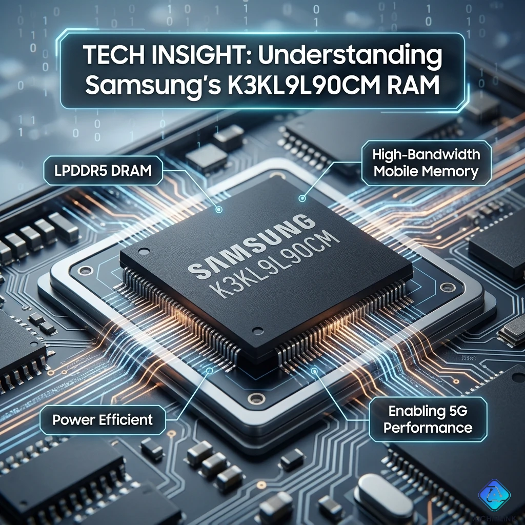
The K3KL9L90CM is Samsung's single-die 64Gb (8GB) LPDDR5X component at 7500 Mbps in a 315-ball FBGA package. One K3KL9L90CM = 8 GB. To build a 12GB system, you would stack two K3KL9L90CM dies (64Gb + 32Gb companion K3KL8L80CM). To build 16GB, you stack two K3KL9L90CM. To build 8GB in the smallest possible footprint with the fewest PCB layers, you use one K3KL9L90CM.
This guide gives you the complete picture: full specifications, part number decoder, power domain architecture, signal integrity design requirements, and the specific pitfalls that appear when engineers push LPDDR5X to 7500 Mbps in production hardware.
1.0 Part Number Decoded: Every Field in K3KL9L90CM-MGCT
Samsung's LPDDR part number system encodes every critical parameter. Here is the full decode for K3KL9L90CM-MGCT:
K3 — Samsung DRAM (K = Samsung semiconductor, 3 = DRAM product category)
K — LPDDR family (K for LPDDR series within Samsung's memory naming)
L — Low-power DRAM type (L = LPDDR)
9 — Generation/speed tier indicator (9 = LPDDR5X generation)
L — Die configuration (L = single die, large density)
9 — Density code (9 = 64Gb per die)
0 — Organization (x32 data bus width per channel, 2-channel architecture)
C — Package type (C = stacked / FBGA configuration)
M — Package variant / ball count tier
-MGCT — Ordering suffix:
- M — Package body size indicator
- G — Temperature grade (G = commercial/mobile: −25°C to +85°C)
- C — Packaging format (C = tray)
- T — Reserved/revision marker
Samsung LPDDR5X family at a glance — closely related dies:
| Part Number | Density | Capacity | Data Rate | Package |
|---|---|---|---|---|
| K3KL9L90CM-MGCT | 64 Gb | 8 GB | 7500 Mbps | 315-FBGA |
| K3KL8L80CM-MGCT | 32 Gb | 4 GB | 7500 Mbps | 315-FBGA |
| K3KL7L70BM-MGCT | 16 Gb | 2 GB | 6400 Mbps | 315-FBGA |
The K3KL9L90CM is the highest-density single-die Samsung LPDDR5X in this family. One die = 8GB of DRAM, delivered through a dual-channel x32 interface (2 channels × 16 bits each, totaling 32 data bits per die).
2.0 Specifications at a Glance
All parameters from Samsung's product page and distributor data for K3KL9L90CM-MGCT:
- Memory Type: LPDDR5X (Low Power Double Data Rate 5X)
- Die Density: 64 Gb (gigabits) = 8 GB (gigabytes)
- Data Bus Organization: x32 (dual-channel × 16-bit per channel)
- Data Rate: 7,500 Mbps per pin (7.5 Gbps)
- Peak Bandwidth (single die, x32): 7,500 Mbps × 32 bits ÷ 8 = 30 GB/s
- JEDEC Standard: JESD209-5B (LPDDR5X)
- Process Technology: 14nm-class (Samsung DRAM process)
- Power Supply Domains:
- VDD1: 1.8V (I/O auxiliary, row precharge)
- VDD2H: 1.05V (core, high-voltage mode)
- VDD2L: 0.9V (core, low-voltage mode — DVFS)
- VDDQ: 0.5V (DQ/DQS data I/O)
- VDDCA: 0.9V (Command/Address bus)
- Operating Temperature: −25°C to +85°C (commercial/mobile grade)
- Package: 315-ball FBGA, approximately 12.4 mm × 15 mm × 1.1 mm
- Channels: 2 independent channels × 16-bit (CA bus shared or independent depending on SoC)
- Bank Architecture: 8 banks per channel (16 total), 4 bank groups per channel
- Burst Length: BL16 (16n prefetch; LPDDR5X uses 16n prefetch vs LPDDR5's 16n)
- Read Latency: Configurable; typically RL = 36–46 cycles at 7500 Mbps
- Power-saving features: DVFS (Dynamic Voltage and Frequency Scaling), DQ Copy, WriteX, deep power-down, partial array self-refresh (PASR), temperature-compensated self-refresh (TCSR)
- ZQ Calibration: On-die ZQ via external 240Ω ± 1% reference resistor
- RoHS / Halogen-Free: Yes
8GB in context: A single K3KL9L90CM die delivers 30 GB/s of bandwidth. To put this in perspective — the peak memory bandwidth of the first Apple M1 chip is 68.25 GB/s using two LPDDR5 channels at 6400 Mbps. A system using two K3KL9L90CM at 7500 Mbps delivers approximately 60 GB/s — approaching that same figure from one LPDDR5X generation later.
3.0 How LPDDR5X Works at 7500 Mbps
From LPDDR5 to LPDDR5X — what actually changed:
LPDDR5X ("Extended" or "eXtended") pushes the same LPDDR5 physical interface beyond its original 6400 Mbps ceiling. The key architectural changes that enable 7500 Mbps (and higher) in LPDDR5X:
Improved signal integrity: LPDDR5X tightens the AC timing margins in the JEDEC specification, requiring improved drive strength and receiver sensitivity at the die level. Samsung's 14nm-class process enables the finer-pitched transistors needed for these tighter margins.
Enhanced DFE/DQ equalizer: Decision Feedback Equalization on the DQ lines compensates for inter-symbol interference (ISI) at 7500 Mbps, where the signal period is only 133 ps — shorter than many PCB trace propagation delays. Without DFE, bit errors would be unacceptably high at this data rate.
DVFS (Dynamic Voltage Frequency Scaling): LPDDR5X supports switching between VDD2H (1.05V, high-performance mode) and VDD2L (0.9V, lower-frequency mode) dynamically. The SoC's memory controller can reduce operating frequency and drop to 0.9V for the core when bandwidth demands are low — a significant power saving in mobile applications where most of the time is spent in light-use scenarios.
DQ Copy and WriteX: Two additional power reduction mechanisms. DQ Copy reduces power during reads by copying data from one data group to another instead of re-driving the bus. WriteX (Write Execute) bundles multiple writes for more efficient NAND-like block writes, reducing switching activity.
Dual-channel architecture on a single die:
The K3KL9L90CM presents two independent 16-bit channels (Channel A and Channel B) to the host SoC. These channels share the same die but have independent CA (Command/Address) buses and DQ (Data) buses. The SoC memory controller can operate them simultaneously (for full 32-bit bandwidth) or independently (for lower-power operation on one channel at a time).
This dual-channel-per-die architecture is what makes LPDDR5X so powerful for mobile AI applications: the SoC can sustain 30 GB/s through a single die while accessing different addresses in each channel simultaneously, supporting the memory access patterns of neural network inference workloads.
CA bus — the training-intensive part:
Unlike DDR5 which uses a fly-by topology, LPDDR5X uses a point-to-point CA bus. The 6-bit CA bus carries command and address information at DDR rate (the CA bus runs at half the data rate — 3750 MHz for 7500 Mbps data). Proper CA training, write leveling, and DQ calibration are mandatory before the memory subsystem is operational. On Samsung LPDDR5X, this initialization sequence typically takes 2–5 ms from power-on to first available read/write access.
4.0 ⚠️ Five Pitfalls That Break LPDDR5X Designs at 7500 Mbps
Pitfall 1: VDDQ at 0.5V is not the same as LPDDR5's 0.5V VDDQ — different noise budget
LPDDR5X tightens the DQ signal eye diagram requirements compared to LPDDR5 at the same 0.5V VDDQ. A VDDQ LDO designed with 50 mV of output ripple tolerance for LPDDR5 may cause intermittent read errors on LPDDR5X at 7500 Mbps. The reason: the DQ signal amplitude is 0.5 × VDDQ = 0.25V per swing. At 50 mV VDDQ ripple, the eye opening is reduced by 10% of the nominal DQ swing — measurable margin loss that becomes bit errors under thermal stress. Fix: use a VDDQ LDO with maximum 20 mV output ripple, decouple with 10 µF + 100 nF at each VDDQ ball cluster.
Pitfall 2: Insufficient decoupling on VDD2H causes core brownouts during burst writes
VDD2H (1.05V) powers the DRAM core array. During burst write operations, the current drawn from VDD2H spikes at 200–400 mA within a few nanoseconds — faster than the slew rate of most LDO outputs. If bulk decoupling on VDD2H is insufficient (< 47 µF), the voltage droops below the minimum 1.0V specification during these spikes. The DRAM controller detects the violation and triggers a reset — appearing as a random hang or memory controller timeout. This failure is thermal-dependent: it occurs most often at elevated temperature when LDO output impedance increases. Fix: place at least 47 µF (two 22 µF X5R capacitors) within 5 mm of the VDD2H ball cluster, plus 100 nF per ball.
Pitfall 3: PCB trace impedance mismatch causes DQ eye closure at 7500 Mbps
At 7500 Mbps, each bit period is 133 ps. A 1% impedance mismatch on a DQ trace causes a reflection that arrives 0.5–1 bit periods later — directly corrupting the following bit at this data rate. Many PCB fabrication vendors specify ±10% impedance tolerance on standard processes. This is adequate for LPDDR4X at 4266 Mbps but insufficient for LPDDR5X at 7500 Mbps. Fix: specify ±5% impedance tolerance in your PCB fabrication notes for all LPDDR5X signal layers. This typically requires tighter width/dielectric control and may add cost. Validate with a time-domain reflectometer (TDR) measurement on fabricated boards before committing to production.
Pitfall 4: Skipping CA training because "it worked in simulation"
SPICE simulation with idealized transmission line models at 7500 Mbps consistently shows clean CA eye diagrams. Real PCBs have dielectric inhomogeneities, via stubs, connector reflections, and glass-weave effect that are not captured in most pre-layout simulations. Engineers who skip CA training in firmware (or implement it incompletely) and rely on simulation sign-off discover in silicon bring-up that command-level errors cause the memory controller to issue incorrect row/bank addresses — resulting in data corruption that is indistinguishable from software bugs. Always implement the full Samsung-specified CA training, write leveling, and DQ calibration sequence in your bring-up firmware, regardless of simulation results.
Pitfall 5: Using a single ZQ calibration at initialization without periodic ZQ updates
ZQ calibration adjusts the DRAM's output driver impedance and ODT impedance to compensate for process, voltage, and temperature variation. Samsung's K3KL9L90CM specification requires ZQ calibration at initialization (ZQCAL_LONG) and periodic short ZQ calibrations (ZQCAL_SHORT) during operation. An SoC memory controller configured for ZQCAL_LONG only at boot will show degraded signal integrity after 30–60 minutes of operation as the die temperature rises. Drive strength and ODT values drift with temperature; without periodic re-calibration, the DQ eye opening narrows until bit errors appear. Fix: configure your SoC memory controller to issue ZQCAL_SHORT every 128 ms (or per the datasheet recommendation), particularly critical for mobile devices where the SoC+DRAM temperature can rise by 30–40°C during sustained computational load.
5.0 PCB and System Design Notes
Package and footprint:
315-ball FBGA, approximately 12.4 mm × 15 mm body, 0.65 mm ball pitch. The FBGA is not the same as TFBGA (thin FBGA used in eMMC) — LPDDR5X uses a thicker package body with more routing layers internally to accommodate the higher pin density and signal integrity requirements of the high-speed differential pairs.
PCB layer requirements:
A minimum 8-layer PCB is strongly recommended for LPDDR5X at 7500 Mbps: the signal routing requires at least two dedicated signal layers for DQ/DQS (one per channel), plus reference planes immediately above and below each signal layer for impedance control. A 6-layer board can work for low-complexity single-die configurations at 6400 Mbps but is marginal at 7500 Mbps due to limited reference plane options.
Signal routing rules for 7500 Mbps:
- Target trace impedance: 40 Ω (±5%) for DQ/DQS single-ended; 80 Ω (±5%) differential for DQS pairs
- Maximum trace length (SoC to DRAM): 25–35 mm — shorter traces reduce insertion loss and reflect less at 7500 Mbps
- Intra-byte DQ-to-DQS length matching: ±5 mil (0.127 mm)
- Inter-byte DQ group length matching: ±100 mil (2.54 mm)
- CA bus matching: ±20 mil across all CA bits — less critical than DQ but still required
- No stubs, no 90° bends; avoid via transitions in DQ routing if possible; if vias are required, use backdrill to remove via stubs
Power domain decoupling summary:
| Domain | Voltage | Bulk Cap | Per-Ball Bypass | Placement |
|---|---|---|---|---|
| VDD1 | 1.8V | 22 µF | 100 nF | Within 5 mm |
| VDD2H | 1.05V | 47 µF | 100 nF per ball | Within 3 mm |
| VDD2L | 0.9V | 22 µF | 100 nF | Within 5 mm |
| VDDQ | 0.5V | 22 µF | 100 nF per ball | Within 2 mm |
| VDDCA | 0.9V | 22 µF | 100 nF | Within 5 mm |
ZQ reference resistor:
Connect a 240 Ω ± 1% thin-film resistor from the ZQ ball to VSS, placed within 15 mm of the ZQ ball. Use thin-film (not thick-film) for the ±1% tolerance requirement — thick-film resistors are typically ±5% and will degrade calibration accuracy.
6.0 Comparison: When to Use K3KL9L90CM vs Alternatives
| Scenario | K3KL9L90CM (single 64Gb die) | 2× K3KL8L80CM (2× 32Gb dies) | LPDDR5 (6400 Mbps) | SK Hynix H9JCNNNFA5MLNR-JP0 |
|---|---|---|---|---|
| Total capacity | 8 GB | 8 GB | 8 GB (typical) | 8 GB (LPDDR5X) |
| Data rate | 7500 Mbps | 7500 Mbps | ≤6400 Mbps | 7500 Mbps |
| Peak BW (system) | 30 GB/s | 30 GB/s | ~25 GB/s | 30 GB/s |
| PCB footprint | 1 BGA package | 2 BGA packages | 1–2 packages | 1 BGA package |
| PCB routing complexity | Single location | Two separate placements | Lower (lower freq) | Similar |
| BOM cost | Reference | Slightly higher | Lower | Comparable |
| DVFS support | Yes | Yes | Yes | Yes |
| Best for | Compact 8GB systems | Flexible 4+4 capacity split | Power-constrained designs | Samsung/SK Hynix dual-source |
When NOT to use K3KL9L90CM:
- You need 12GB or 16GB — use multiple dies or a different package configuration
- Your SoC is only validated for LPDDR5 6400 Mbps and does not support 7500 Mbps operation
- Your PCB cannot meet ±5% impedance tolerance (limited fabrication capability) — the 6400 Mbps LPDDR5 die has more margin at lower data rate
- Your system operates above +85°C — the commercial grade K3KL9L90CM-MGCT is not rated above +85°C; use an automotive-qualified LPDDR5X variant if available
7.0 Sourcing Authentic K3KL9L90CM
Authorized distribution: K3KL9L90CM-MGCT is a Samsung production component. Samsung's authorized semiconductor distributors include Arrow Electronics, Avnet, and Samsung's own component distribution channels. DigiKey and Mouser may carry Samsung DRAM components in their catalog.
Counterfeit risk: High-speed mobile DRAM dies are among the most counterfeited components in the secondary market. A counterfeited K3KL9L90CM may operate at lower speeds (a 6400 Mbps LPDDR5 die remarked as 7500 Mbps LPDDR5X), have lower density (a 32Gb die in a package marked as 64Gb), or fail entirely at 7500 Mbps while appearing functional at lower speeds during initial testing.
How to verify authenticity:
- Read the MR (Mode Register) on initialization: the DRAM's MR8 register returns the manufacturer ID and die density. Samsung LPDDR5X should return manufacturer code 0x01 (Samsung) and the correct density code for 64Gb.
- Run the full 7500 Mbps validation test suite from your SoC's memory validation toolkit — genuine Samsung K3KL9L90CM passes at rated speed; remarked LPDDR5 dies fail above ~6400 Mbps.
- Request a Certificate of Conformance with Samsung lot traceability from your distributor.
For verified authentic Samsung K3KL9L90CM inventory with competitive pricing and full traceability, visit aichiplink.com.
8.0 Real Questions from Mobile and Embedded Designers
Q: My SoC datasheet says it supports "LPDDR5X up to 6400 Mbps." Can I use K3KL9L90CM-MGCT at 6400 Mbps?
A: Yes. LPDDR5X is backward-compatible with lower data rates. The K3KL9L90CM at 7500 Mbps is Samsung's rated maximum, but the die operates at any speed from LPDDR5X's minimum up to 7500 Mbps. If your SoC's memory controller is qualified to 6400 Mbps, you configure the frequency accordingly and the K3KL9L90CM operates at that speed without issue — you simply do not use the upper 15% of its bandwidth capability. This is a common configuration: system vendors use the highest-speed available LPDDR5X die to ensure margin at the SoC's maximum supported rate, even if the DRAM die itself is rated higher.
Q: I need to design a system with 12GB of LPDDR5X. Can I achieve this with K3KL9L90CM and another die?
A: Yes. A 12GB configuration typically stacks one 64Gb (8GB) K3KL9L90CM die and one 32Gb (4GB) K3KL8L80CM die in a package-on-package (PoP) or side-by-side configuration, depending on your SoC's memory controller support. However, mixed-density configurations require the memory controller to handle two differently-sized DRAM regions, which some SoC controllers support natively and others require specific firmware initialization sequences to configure correctly. Verify your specific SoC's support for asymmetric LPDDR5X configurations before committing to this topology.
Q: The power-up sequence for LPDDR5X looks complex — VDD1 before VDD2H before VDDQ. What happens if VDD2H rises before VDD1?
A: Applying VDD2H before VDD1 can latch up the DRAM's internal circuits. VDD1 (1.8V) must be stable before VDD2H (1.05V) begins ramping. The JEDEC LPDDR5X specification defines the required power-up sequence with specific maximum ramp rates and sequencing windows. Most PMIC (Power Management IC) solutions designed for mobile SoC platforms implement this sequencing in hardware — the PMIC's internal power-on sequence ensures correct rail ordering. If you are designing a custom PMIC configuration or discrete LDO solution, implement a sequencer IC (such as a programmable multi-rail sequencer) to guarantee the required ordering. A violated power-up sequence that causes latch-up will damage the DRAM die permanently.
Q: K3KL9L90CM shows "active" status on Samsung's site but also mentions "no matches were found" in product details. Is this part being discontinued?
A: The "no matches were found" message on Samsung Semiconductor's product detail page reflects a search or content limitation on their web interface, not product status. The K3KL9L90CM is confirmed as an active Samsung product in authorized distributor listings (DigiKey, Mouser, Arrow) as of 2025. Samsung updates product detail pages in batches and some pages may show content loading issues without reflecting product lifecycle status. For definitive lifecycle status, use Samsung's authorized distributor channels or contact Samsung's memory FAE (Field Application Engineer) directly. Do not make production lifecycle decisions based on a web interface content error.
9.0 Quick Reference Card
K3KL9L90CM-MGCT at a Glance:
| Parameter | Value |
|---|---|
| Manufacturer | Samsung Semiconductor |
| Type | LPDDR5X |
| Die density | 64 Gb = 8 GB |
| Data rate | 7,500 Mbps per pin |
| Peak bandwidth (x32) | 30 GB/s |
| Channels | 2 × 16-bit (dual-channel) |
| Package | 315-ball FBGA (12.4 × 15 mm) |
| Operating temperature | −25°C to +85°C |
| JEDEC standard | JESD209-5B (LPDDR5X) |
Five Power Domains — At a Glance:
| Domain | Voltage | Function | Min Bulk Cap |
|---|---|---|---|
| VDD1 | 1.8V | I/O auxiliary | 22 µF |
| VDD2H | 1.05V | Core (high-perf) | 47 µF |
| VDD2L | 0.9V | Core (DVFS low) | 22 µF |
| VDDQ | 0.5V | DQ/DQS I/O | 22 µF + 100nF/ball |
| VDDCA | 0.9V | CA bus | 22 µF |
Power-up sequence: VDD1 → VDD2H/VDD2L → VDDCA → VDDQ → deassert reset → CA training
PCB Rules for 7500 Mbps:
| Parameter | Requirement |
|---|---|
| DQ/DQS impedance | 40 Ω single-ended, ±5% |
| DQS differential impedance | 80 Ω, ±5% |
| Max trace length (SoC to DRAM) | 25–35 mm |
| Intra-byte DQ-DQS matching | ±5 mil |
| ZQ reference resistor | 240 Ω ±1% thin-film to VSS |
| PCB layers (minimum) | 8 layers |
Samsung LPDDR5X Die Family (same 315-FBGA footprint):
| Part | Density | System Cap | Max Speed |
|---|---|---|---|
| K3KL7L70BM-MGCT | 16 Gb | 2 GB | 6400 Mbps |
| K3KL8L80CM-MGCT | 32 Gb | 4 GB | 7500 Mbps |
| K3KL9L90CM-MGCT | 64 Gb | 8 GB | 7500 Mbps |
For sourcing Samsung K3KL9L90CM-MGCT and related LPDDR5X memory components with verified authenticity and competitive pricing, visit aichiplink.com.

Written by Jack Elliott from AIChipLink.
AIChipLink, one of the fastest-growing global independent electronic components distributors in the world, offers millions of products from thousands of manufacturers, and many of our in-stock parts is available to ship same day.
We mainly source and distribute integrated circuit (IC) products of brands such as Broadcom, Microchip, Texas Instruments, Infineon, NXP, Analog Devices, Qualcomm, Intel, etc., which are widely used in communication & network, telecom, industrial control, new energy and automotive electronics.
Empowered by AI, Linked to the Future. Get started on AIChipLink.com and submit your RFQ online today!
Frequently Asked Questions
What is K3KL9L90CM?
K3KL9L90CM is a 64Gb (8GB) LPDDR5X DRAM die from Samsung, supporting up to 7500 Mbps data rate with a dual-channel x32 interface, designed for high-performance mobile and AI applications.
How much memory does K3KL9L90CM provide?
K3KL9L90CM provides 8GB of memory per die, making it ideal for smartphones, tablets, and embedded systems requiring high bandwidth in a compact footprint.
What is the maximum speed of K3KL9L90CM?
The maximum data rate is 7500 Mbps per pin, delivering up to 30 GB/s bandwidth for a single x32 die configuration.
Can K3KL9L90CM run at lower speeds like 6400 Mbps?
Yes, K3KL9L90CM is backward-compatible with lower LPDDR5X speeds, including 6400 Mbps, depending on the SoC memory controller capability.
What are the key design considerations for K3KL9L90CM?
Critical design factors include power sequencing, impedance control (±5%), CA training, and proper decoupling of VDDQ and VDD2H, especially at 7500 Mbps to ensure signal integrity and system stability.


.png&w=256&q=75)


