There is a story told in electronics education that goes roughly like this: BJTs were the original transistors, then MOSFETs came along, were smaller, consumed less power, scaled better, and over time took over. The story ends with MOSFETs as the obvious modern choice and BJTs as a legacy technology you only encounter in old textbooks.
That story is wrong in an important way.
Walk into any serious RF laboratory and you will find engineers using BJT transistors as their first choice for low-noise amplifiers. Open the schematic of a high-end audio preamplifier and you will find BJTs in the signal path, often deliberately, because their transconductance characteristics produce a specific behavior that MOSFETs do not replicate. Look at the input stage of an op-amp designed for precision voltage sensing and you will find a JFET differential pair selected specifically because its near-infinite input impedance does not disturb the measured signal.
The real picture is not that FETs replaced BJTs. It is that FETs and BJTs each dominate the applications they are physically better suited for, and those domains have relatively little overlap. Understanding which transistor to reach for — and why the physics of each makes it the right choice — is one of the most practically useful things a circuit designer can know.
1.0 The Fundamental Physics: Current Control vs Voltage Control
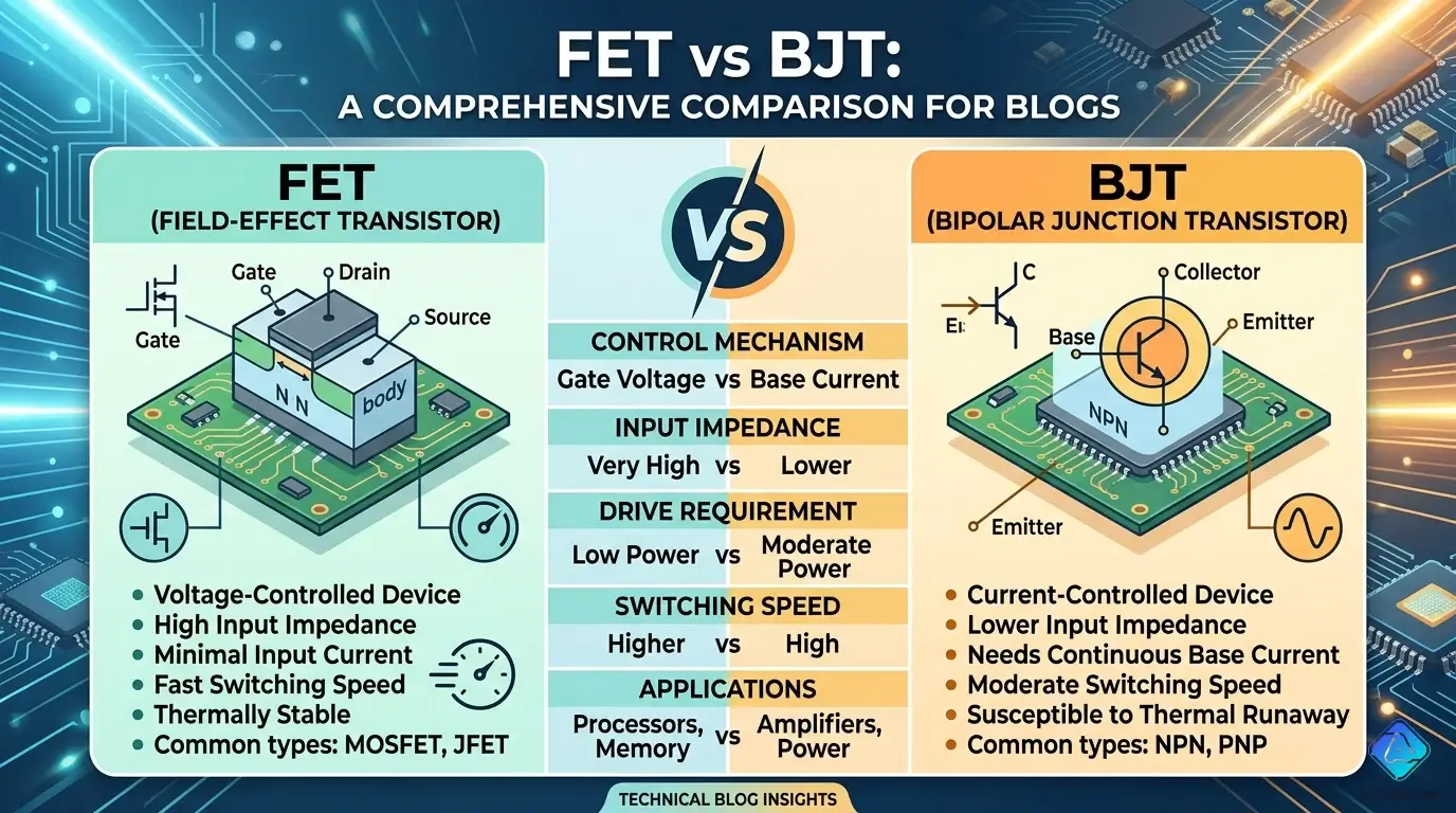
Every important difference between BJTs and FETs traces back to one foundational distinction in how each device is controlled.
The BJT is a current-controlled device. A small current injected into the base terminal controls a larger current flowing between collector and emitter. The relationship is expressed as IC = hFE × IB, where hFE (also called β) is the current gain — typically 100 to 300 for small-signal transistors. This means the BJT draws real current from whatever is driving its base. That driving circuit must supply this base current continuously for the transistor to remain in its operating state.
The FET is a voltage-controlled device. A voltage applied to the gate terminal creates an electric field that modulates the width of a conductive channel between source and drain, controlling current flow without drawing any gate current in steady-state DC operation. The gate is insulated from the channel by either a reverse-biased PN junction (JFET) or a thin oxide layer (MOSFET), giving input impedances on the order of 10⁹ to 10¹⁴ ohms — effectively infinite for practical purposes.
This single difference — current control versus voltage control — explains most of the practical tradeoffs between the two device families:
- Because BJTs require base current, they consume drive power. Because FETs do not, they are more efficient and scale better in digital logic (a CMOS gate dissipates power only during switching transitions, not in steady state)
- Because BJTs are current-driven, their small-signal behavior produces high transconductance (gm) — large changes in output current for small changes in input. This makes them excellent amplifiers
- Because FETs are voltage-driven with near-infinite impedance, they load their source circuit minimally — critical when measuring high-impedance sources like electrodes, piezoelectric sensors, or high-resistance bridges
- Because BJTs use both majority and minority charge carriers (holes and electrons), they are "bipolar" and have faster switching transitions in some respects. FETs use only majority carriers (unipolar), making them more thermally stable
2.0 The Families: Types of BJTs and FETs You Will Actually Encounter
BJT types:
NPN transistor: Current flows from collector to emitter when positive base current is applied. The most common type. Typical parts: 2N3904 (general purpose, 40V/200mA), BC547 (audio, 45V/100mA), 2N2222 (switching, 40V/600mA), MJE3055T (power, 60V/10A).
PNP transistor: Current flows from emitter to collector when negative base current (relative to emitter) is applied. Used as high-side switches and in complementary push-pull output stages. Typical parts: 2N3906 (complement to 2N3904), BC557, MJE2955T.
FET types:
JFET (Junction FET): Gate is a reverse-biased PN junction. Normally ON (depletion mode). Very low noise. Extremely high input impedance. Cannot be fully shut off by gate voltage alone in some configurations. Used in op-amp input stages, audio preamps, and electrometers. Common parts: 2N5457 (N-channel, audio), 2SK170 (N-channel, ultra-low noise), BF245.
MOSFET — Enhancement mode (most common): Gate is insulated by silicon dioxide. Normally OFF. Turned ON by applying VGS above threshold voltage VTH. The dominant type in digital logic and power electronics. Common N-channel parts: 2N7000 (signal level, 60V/200mA), IRF540N (power, 100V/33A), IRFZ44N (power, 55V/49A). Common P-channel: IRF9540, BS250.
MOSFET — Depletion mode: Normally ON, turned OFF by applying gate voltage. Less common. Used in constant current sources and some RF applications.
The IGBT (Insulated Gate Bipolar Transistor): A hybrid device combining the gate-drive simplicity of a MOSFET with the high-voltage, high-current handling of a BJT. Not covered in depth here but worth knowing: IGBTs dominate high-power applications above roughly 600V where MOSFETs become impractical.
3.0 Head-to-Head Parameter Comparison
| Parameter | BJT (NPN small-signal) | JFET (N-channel) | MOSFET (Enhancement N-ch) |
|---|---|---|---|
| Control mechanism | Current (IB) | Voltage (VGS) | Voltage (VGS) |
| Input impedance | Low (1 kΩ – 10 kΩ) | Very high (10⁹ Ω) | Extremely high (10¹² – 10¹⁴ Ω) |
| Gate/Base current | Required (IB = IC/hFE) | ~0 (leakage only) | ~0 (DC) |
| Transconductance (gm) | High (10–100 mA/V at mA bias) | Low–Moderate | Low–Moderate (bias-dependent) |
| Noise (flicker/1/f) | Lower 1/f noise | Low 1/f noise | Higher 1/f noise (MOSFET) |
| Thermal stability | Poor (VBE decreases with temp) | Better | Best (positive temp coefficient of Rds_on helps parallel operation) |
| Switching speed | Fast (but stored charge delays) | Fast | Very fast (majority carrier, no stored charge) |
| On-resistance | Low VCEsat (0.1–0.3V) | Low Rds_on achievable | Very low Rds_on in power MOSFETs |
| Fabrication size | Larger | Smaller | Smallest (CMOS scales to nm) |
| Drive circuit | Requires current source/sink | Simple voltage | Simple voltage (but watch Ciss) |
| Typical applications | Analog amplifiers, RF, audio | Op-amp inputs, audio | Power switching, digital logic, SMPS |
4.0 Where Each Transistor Actually Wins — and Why the Physics Explains It
Where BJTs win: Transconductance-sensitive amplifier circuits
Transconductance (gm) quantifies how much output current a transistor produces per unit of input voltage change. For a BJT biased at a collector current IC:
gm(BJT) = IC / VT
where VT = kT/q ≈ 26 mV at room temperature. At IC = 1 mA: gm = 1 mA / 26 mV = 38.5 mA/V. At IC = 10 mA: gm = 385 mA/V.
For a MOSFET, gm depends on the device geometry and bias: gm(MOSFET) = √(2 × μn × Cox × W/L × ID). For a typical small-signal MOSFET at 1 mA: gm ≈ 1–5 mA/V — roughly 10 to 40 times lower than a BJT at the same current.
This is why discrete BJTs dominate audio preamplifier input stages where the highest possible voltage gain from a single stage is needed. The classic 2N3904 biased at 2 mA delivers gm ≈ 77 mA/V, giving a voltage gain of gm × RC with a 1 kΩ collector resistor of about 77 — a respectable gain from a single transistor with no special technology. Achieving similar gain with a MOSFET requires either much larger bias current or a specialized high-gm device.
Where BJTs win: RF low-noise amplifiers below a few GHz
The noise figure of a BJT amplifier at radio frequencies can be lower than an equivalent MOSFET design in the 100 MHz to several GHz range. BJTs have lower 1/f (flicker) noise corner frequencies and excellent noise matching properties in this range. The classic NE85630 (NPN RF transistor, BFR92A, or BFR540) outperforms most MOSFETs in low-noise RF preamplifier designs below 2 GHz. This is why cellular base station low-noise amplifiers (LNAs) used BJTs for decades and still commonly use heterojunction bipolar transistors (HBTs — an advanced BJT variant) in high-frequency designs.
Where FETs win: Nearly everything in digital logic and power switching
In digital CMOS logic, a FET draws essentially zero gate current in steady state. This means a single logic gate output can drive thousands of CMOS gate inputs without any loading concern — enabling the massive fan-out that makes complex ICs practical. If gates were BJT-driven, each load gate would require base current, rapidly overwhelming any driver stage. CMOS logic dissipates power only during switching (charging and discharging gate capacitance), not in static DC states — which is the foundation of modern low-power digital design.
In power switching applications (motor drives, DC-DC converters, inverters), MOSFETs offer a decisive thermal stability advantage. As a MOSFET heats up, its on-resistance (Rds_on) increases — which reduces current through the device, providing a self-limiting mechanism that prevents thermal runaway. BJTs exhibit the opposite behavior: as temperature rises, current gain increases, which increases current, which increases dissipation, which increases temperature further. This positive feedback loop is thermal runaway and is why parallel BJTs in power stages require emitter degeneration resistors for stabilization. MOSFETs connected in parallel naturally share current more evenly as temperature varies.
Where JFETs win: Ultra-high impedance signal acquisition
For measuring signals from sources with very high impedance — a pH electrode (50–500 MΩ), a piezoelectric sensor, an ionization chamber, or a photodiode in current mode — the input stage must draw essentially zero current. JFET input op-amps (OPA132, LF411, TL071) offer input bias currents of 50–100 pA, compared to 50–200 nA for BJT input op-amps. At a source impedance of 100 MΩ, a 100 pA input current creates 10 mV of error — already significant. A 100 nA BJT input current would create 10 V of error, saturating the amplifier entirely.
5.0 ⚠️ Three Circuit Design Mistakes That Come From Choosing the Wrong One
Mistake 1: Using a MOSFET where a BJT was needed because "MOSFETs are modern"
A common mistake in audio amplifier design is replacing BJTs with MOSFETs because MOSFETs seem more contemporary and are easier to drive (no base current required). The result is often a design that works but has noticeably lower voltage gain from each stage, requiring more stages to achieve the same overall amplification. Worse, at low bias currents, the MOSFET gm is so low that the amplifier's noise performance degrades. A 2N3904 BJT biased at 1 mA delivers gm ≈ 38 mA/V; swapping it for a 2N7000 MOSFET at the same current delivers gm of roughly 1–3 mA/V. The gain drops by a factor of 10 to 30. Fix: use BJTs in the signal path wherever high transconductance and low noise at modest currents are the priority; use MOSFETs in the power output stage where their switching efficiency, thermal stability, and ease of gate drive are genuinely advantageous.
Mistake 2: Connecting power BJTs in parallel without emitter resistors
Power BJTs share a destructive thermal characteristic: as junction temperature rises, the base-emitter voltage VBE decreases (at approximately −2 mV/°C), which increases collector current for the same base drive. More current means more dissipation, which raises temperature further. When two BJTs are connected in parallel and one is slightly hotter (due to die variation or thermal resistance differences), it carries more current, gets hotter, carries even more current, and in extreme cases enters thermal runaway. The standard fix is to add a small emitter degeneration resistor (typically 0.1–0.47 Ω) in each emitter leg, which provides local negative feedback that stabilizes the current sharing. MOSFETs in parallel do not require this — their positive temperature coefficient of Rds_on provides inherent self-balancing.
Mistake 3: Ignoring gate charge in high-frequency MOSFET switching circuits
A MOSFET's gate draws no DC current, which leads some designers to treat gate drive as trivial. At high switching frequencies, this assumption fails badly. The gate input capacitance (Ciss, typically 100–10,000 pF for power MOSFETs) must be charged and discharged on every switching cycle. The peak gate drive current required is:
IG_peak = Ciss × dV/dt = Qg / trise
For a MOSFET with Qg = 50 nC switching in 50 ns: IG_peak = 50 nC / 50 ns = 1 A of instantaneous gate current. A microcontroller GPIO pin rated for 25 mA cannot source this — it will switch the MOSFET slowly, increasing switching losses and potentially destroying both devices. Fix: always use a dedicated gate driver IC (UCC27321, TC4420, IR2104) between the logic control signal and any power MOSFET gate. BJTs are rarely used directly in power switching for this reason; when they are, a dedicated base driver network is required.
6.0 Decision Guide: The Right Transistor for Your Application
Use a BJT (NPN or PNP) when:
- Maximum transconductance from a single stage at moderate bias current is needed (audio preamplifiers, instrumentation amplifiers)
- Low-noise RF amplification below 2–3 GHz (use RF-grade BJT like BFR540, MRF901, or modern SiGe HBT)
- Simple, low-part-count switching of small loads (< 500 mA) where base current can come from a microcontroller pin directly through a resistor
- Precise voltage reference or bandgap-based circuits (VBE temperature coefficient is well-characterized and used in bandgap references)
- Complementary push-pull output stages in class-AB audio amplifiers where NPN/PNP symmetry is needed
Use a MOSFET (N-channel or P-channel) when:
- Power switching: motor drivers, SMPS, inverters, H-bridges — especially above 1 A where MOSFET on-resistance and thermal stability dominate
- Digital logic interface and level shifting
- Battery-powered designs where zero quiescent gate current matters
- High-frequency switching above 100 kHz (MOSFET's lack of minority carrier storage means faster transitions)
- Multiple devices in parallel (Rds_on positive temperature coefficient provides self-balancing)
- Any application where gate drive current is unavailable or inconvenient
Use a JFET when:
- Extremely high input impedance is required in an analog front end (electrometers, pH meters, piezo sensing)
- Low 1/f noise in audio circuits at the very lowest frequencies (JFET 1/f corner is typically lower than MOSFET)
- Voltage-controlled resistor applications (JFET in its ohmic region acts as a voltage-controlled resistor — useful in automatic gain controls and variable attenuators)
- Simple current sources with few components (JFET with gate tied to source self-biases at IDSS)
When NOT to use a BJT: High-density digital logic (scaling is poor), battery-powered microcontroller circuits where the base current draw reduces standby battery life, any power stage above a few hundred milliamperes where thermal runaway risk needs management.
When NOT to use a MOSFET: Where maximum gain per stage is the priority with limited bias current, RF low-noise amplification in the 100 MHz–3 GHz range where BJT noise figures are lower, simple indicator LED drivers from MCU pins (a 2N3904 with a base resistor is simpler than a MOSFET gate drive network).
7.0 Common Parts and Where to Source Them
Most widely used BJTs for new designs:
| Part | Type | Key specs | Typical use |
|---|---|---|---|
| 2N3904 | NPN | 40V, 200mA, hFE 100–300 | General purpose, audio, switching |
| 2N3906 | PNP | 40V, 200mA | Complement to 2N3904 |
| BC547B | NPN | 45V, 100mA, low noise | Audio signal path |
| 2N2222A | NPN | 40V, 600mA | Switching, driver |
| BFR92A | NPN RF | 15V, 25mA, fT 5 GHz | RF LNA, VHF/UHF |
| MJE3055T | NPN Power | 60V, 10A | Power amplifier output |
Most widely used FETs for new designs:
| Part | Type | Key specs | Typical use |
|---|---|---|---|
| 2N7000 | N-ch MOSFET | 60V, 200mA, logic-level | Signal switching, MCU interface |
| IRF540N | N-ch Power MOSFET | 100V, 33A, Rds_on 44 mΩ | Motor driver, SMPS |
| IRFZ44N | N-ch Power MOSFET | 55V, 49A, Rds_on 17.5 mΩ | High-current switching |
| BS170 | N-ch MOSFET | 60V, 500mA | Small signal switching |
| 2SK170 | N-ch JFET | −30V, 20mA, ultra-low noise | Audio preamp input stage |
| 2N5457 | N-ch JFET | 25V, 10mA | Audio, VCR, general analog |
All of the above are available from Mouser, DigiKey, and Arrow in authorized stock. For competitive pricing on both BJT and FET components with verified traceability, visit aichiplink.com.
8.0 Real Questions from Circuit Designers
Q: I am designing a simple circuit to turn on a 12V relay from a 3.3V microcontroller GPIO. Should I use a 2N3904 BJT or a 2N7000 MOSFET?
A: Either works, but the 2N3904 BJT is the simpler choice for this specific application. Add a 1 kΩ base resistor from the GPIO pin to the base (this limits base current to about 3.3V/1 kΩ = 3.3 mA, which with hFE of 100 gives collector current capacity of 330 mA — more than enough for a typical relay coil at 50–100 mA). Add a flyback diode across the relay coil. Total component count: transistor, resistor, diode. For the 2N7000 MOSFET approach, the threshold voltage is specified up to 3V, which leaves very little margin when driving from a 3.3V GPIO. A logic-level MOSFET like the FQP30N06L (VGS(th) maximum 2.5V) would be safer, but adds more complexity. For a simple relay driver from a 3.3V or 5V MCU, a BJT with base resistor is the most reliable, lowest-part-count solution.
Q: Why does my class-AB audio amplifier's output transistors (NPN/PNP BJT pair) get hot unevenly — one transistor always runs hotter than the other?
A: Most likely cause is an imbalanced bias point or a slight mismatch in transistor parameters (VBE at the operating current). In a complementary BJT push-pull output stage, if the quiescent current (set by the VBE multiplier bias circuit) is not centered correctly between the two transistors, one transistor handles more of the idle current than the other. Check that the bias voltage across the two output transistors at idle produces equal emitter currents in both. Thermal coupling between the VBE multiplier transistor and the output transistors (mounting the VBE multiplier on the heatsink) is essential — if the multiplier is at a different temperature than the outputs, the thermal compensation does not work correctly. Also verify that both output transistors have emitter degeneration resistors of equal value — they must be present and matched to within 5%.
Q: Can I use a MOSFET as a linear regulator pass element instead of a BJT? Some regulators use BJTs, some use MOSFETs.
A: Yes, and both approaches are common. The choice affects several design parameters. A MOSFET pass element typically offers lower dropout voltage in low-dropout (LDO) regulators because Vds(sat) can be much lower than BJT's VCEsat — enabling regulators that function with input-output differential of only 100–200 mV. However, MOSFETs in linear mode (partially on, dissipating power) can be thermally tricky: their Rds_on increases with temperature, but in a linear regulator the device is not operating in its resistive region — it operates in saturation, where the same thermal runaway risk that affects BJTs can also affect MOSFETs under certain conditions. Modern CMOS LDO regulators handle this through careful design. For most applications, a well-designed IC LDO regulator (LP2985, AMS1117, TLV1117) solves the problem for you without needing to select the pass transistor yourself.
Q: I've seen the 2SK170 JFET recommended for high-end audio preamps but it's expensive and hard to find. Can I substitute a MOSFET?
A: The 2SK170 is prized in audio circuits for its very low noise (noise voltage as low as 0.75 nV/√Hz at 1 kHz), high transconductance for a JFET (gm up to 40 mA/V at 10 mA), and low 1/f noise corner frequency. Direct MOSFET substitution is difficult because most enhancement-mode MOSFETs have significantly higher 1/f noise (the oxide interface creates additional noise sources) and lower gm at similar bias currents. The BSS170 and similar small-signal MOSFETs are not drop-in equivalents for noise performance. For new designs, the 2SK170 is effectively obsolete (Toshiba discontinued it), but the LSK170 from Linear Integrated Systems is a direct equivalent in current production. Alternatively, the BF862 (NXP/Nexperia) is an N-channel JFET with comparable noise performance (0.85 nV/√Hz) and is actively manufactured. Both are significantly better choices than a MOSFET for a high-performance audio input stage.
9.0 Quick Reference Card
Control Mechanism Summary:
| BJT | JFET | MOSFET | |
|---|---|---|---|
| Controlled by | Base current IB | Gate voltage VGS | Gate voltage VGS |
| Input impedance | ~1–10 kΩ | ~10⁹ Ω | ~10¹² – 10¹⁴ Ω |
| Gate/Base current needed | Yes (IB = IC/hFE) | No (leakage only) | No (DC) |
Transconductance at Common Bias Points:
| Bias Current | BJT gm | MOSFET gm (typical) |
|---|---|---|
| 0.1 mA | ~3.8 mA/V | ~0.1–0.5 mA/V |
| 1 mA | ~38.5 mA/V | ~1–5 mA/V |
| 10 mA | ~385 mA/V | ~3–15 mA/V |
BJT transconductance at 1 mA is 5–40× higher than a typical MOSFET at the same current.
Application Domain Summary:
| Application | Best Choice | Reason |
|---|---|---|
| Audio signal amplification | BJT | Highest gm, lowest noise at signal currents |
| RF LNA (< 3 GHz) | BJT / SiGe HBT | Lower noise figure, better noise matching |
| Power switching (> 1A) | MOSFET | Thermal stability, Rds_on, easy gate drive |
| Digital logic / CMOS | MOSFET | Zero quiescent power, scaling, fan-out |
| High-impedance sensing | JFET | Near-infinite input impedance, low bias current |
| Simple MCU relay driver | BJT (with base R) | Low part count, adequate for most loads |
| 100 kHz+ switching | MOSFET | No minority carrier storage, faster transitions |
| Parallel power stage | MOSFET | Positive Rds_on tempco enables self-balancing |
The one-sentence rule:
Choose BJT when you need maximum gain per milliamp of bias current. Choose MOSFET when you need maximum efficiency, high input impedance, or integrated circuit compatibility.
For sourcing discrete BJT and FET transistors including 2N3904, BC547, IRF540N, 2N7000, and JFET types, visit aichiplink.com.

Written by Jack Elliott from AIChipLink.
AIChipLink, one of the fastest-growing global independent electronic components distributors in the world, offers millions of products from thousands of manufacturers, and many of our in-stock parts is available to ship same day.
We mainly source and distribute integrated circuit (IC) products of brands such as Broadcom, Microchip, Texas Instruments, Infineon, NXP, Analog Devices, Qualcomm, Intel, etc., which are widely used in communication & network, telecom, industrial control, new energy and automotive electronics.
Empowered by AI, Linked to the Future. Get started on AIChipLink.com and submit your RFQ online today!
Frequently Asked Questions
What is the main difference between FET and BJT?
The key difference is control mechanism: BJTs are current-controlled devices, while FETs are voltage-controlled, resulting in higher input impedance and lower power consumption for FETs.
Which is better for switching applications: FET or BJT?
MOSFETs are generally better for switching, especially in power and high-frequency circuits, due to faster switching speed, higher efficiency, and better thermal stability.
Why are BJTs still used in modern circuits?
BJTs offer higher transconductance and lower noise, making them ideal for audio amplifiers, RF circuits, and precision analog designs.
When should I use a MOSFET instead of a BJT?
Use a MOSFET when you need high efficiency, low power consumption, high input impedance, or fast switching, such as in SMPS, motor drivers, and digital circuits.
Can a MOSFET replace a BJT in all applications?
No. While MOSFETs dominate digital and power electronics, BJTs still outperform in high-gain analog and low-noise applications, so replacement depends on the specific circuit requirements.