What Is 5PB1108PGGK8? Why a Clock Buffer Is Not Just a Wire With Eight Endpoints
The most direct explanation of what a clock fanout buffer does — "it takes one clock signal and copies it to eight outputs" — is technically accurate but misses the reason clock fanout buffers exist. A resistor network can also route one signal to eight endpoints. A PCB trace with eight branches can also connect one source to eight destinations. Neither of these substitutes for a dedicated clock buffer, and understanding why is the key to understanding what the Renesas 5PB1108PGGK8 provides.
The problem with passive branching is loading. Every device connected to a clock signal presents a capacitive load. When a crystal oscillator or PLL output drives eight devices through a passive network, it drives the sum of all eight loads simultaneously. The rise and fall times of the clock edge slow down, the output drive capability of the source is exceeded, and the clock signal degrades — wider transitions, higher jitter, and signal integrity that varies with how many devices are present and what each one's input capacitance is.
A clock buffer solves this by breaking the dependency between the source drive capability and the load count. The buffer's input presents a single, well-defined load to the clock source. The buffer's internal driver then regenerates the clock signal — new edges with full drive strength — and presents that regenerated signal to each of the eight outputs independently. The source never "sees" the eight loads; it sees only the buffer input. Each output drives its own independent load without affecting the others.
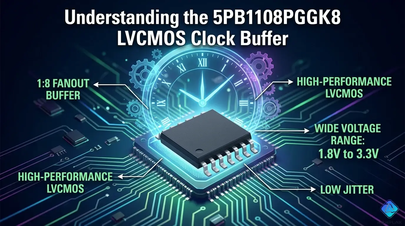
The 5PB1108PGGK8 is Renesas's implementation of a 1:8 LVCMOS clock fanout buffer optimized for exactly this application: distributing a single LVCMOS clock signal to eight endpoints with matched propagation delay, controlled output skew, and support for supply voltages from 1.8V to 3.3V.
1.0 Part Number Decoded: 5PB1108PGGK8
Renesas (via the IDT/Integrated Device Technology heritage) uses a structured naming convention for their clock distribution products:
5PB — Product family prefix:
- 5 = 5-series LVCMOS clock buffer family from IDT (now Renesas)
- PB = Low-Power Buffer (as opposed to 5PC, 5PD, etc., for other feature combinations)
1108 — Device identifier:
- 11 = device class within the 5PB buffer family
- 08 = 1:8 fanout ratio — one input, eight outputs
- Compare: 5PB1104 = 1:4 fanout; 5PB1108 = 1:8 fanout
PGG — Package code:
- P = plastic package
- GG = TSSOP (Thin Shrink Small Outline Package) in Renesas's IDT coding
K — Temperature grade:
- K = Commercial temperature: 0°C to +70°C (some Renesas sources list the commercial range as 0°C to +85°C — verify against the current datasheet)
- I = Industrial temperature: −40°C to +85°C → the industrial variant is 5PB1108PGGI8
8 — Pin count: 8 pins total (TSSOP-8)
Part family context:
| Device | Fanout | Package | Temperature |
|---|---|---|---|
| 5PB1104PGGK8 | 1:4 | TSSOP-8 | Commercial |
| 5PB1108PGGK8 | 1:8 | TSSOP-8 | Commercial |
| 5PB1108PGGI8 | 1:8 | TSSOP-8 | Industrial (−40/+85°C) |
2.0 Specifications: What the 5PB1108 Provides
From the Renesas 5PB1108 datasheet (DS-1108-001):
Electrical:
- Fanout: 1:8 (one input, eight outputs)
- Logic standard: LVCMOS input, LVCMOS output
- Supply voltage (VCC): 1.8V, 2.5V, or 3.3V — the device operates across this range and its output levels track VCC
- Maximum input frequency: 200 MHz
- Output drive: LVCMOS levels with sufficient drive to maintain signal integrity driving typical PCB loads
Timing performance:
- Propagation delay (tPD): approximately 1.5–4 ns (input to output, varies with VCC and load — lower at 3.3V, slightly higher at 1.8V)
- Output skew (tSK): typically < 250 ps — the maximum time difference between the earliest and latest output transition across all 8 outputs simultaneously
- Output-to-output skew: typically < 100 ps (between any two outputs under identical conditions)
- Rise/fall time: approximately 1–3 ns (10%–90%, load-dependent)
- Additive jitter: very low — the buffer does not significantly degrade the input clock's jitter
Other features:
- Output Enable (OE): Active-high enable; when OE is low, all outputs are tri-stated (high-impedance) — useful for power-down, board-level test, or clock gating
- Input: single-ended LVCMOS; the input has a high input impedance so it loads the clock source minimally
Power:
- Quiescent current (ICC): typically 5–15 mA depending on VCC and switching frequency
- Low-power family: The 5PB series is optimized for power consumption relative to other IDT/Renesas clock buffer families
Package:
- TSSOP-8 (Thin Shrink Small Outline Package), 3mm × 4.4mm body, 0.65mm lead pitch
- 8 pins: VCC, GND, CLK input, OE, and 4 outputs (note: with 8 outputs and only 8 pins total, verify datasheet for exact pin assignment — the 5PB1104 is 1:4 in TSSOP-8; the 5PB1108 may use a different package or pin assignment for 8 outputs)
3.0 The Two Key Concepts: Output Skew and Additive Jitter
These two parameters — output skew and additive jitter — define the quality of a clock buffer, and they are independent of each other. Confusing them, or optimizing for one while ignoring the other, leads to clock tree problems that are difficult to diagnose.
Output skew: the between-output timing uncertainty
Output skew is the maximum timing difference between any two output transitions from the same clock buffer, measured at the same voltage threshold, when all outputs are switching simultaneously. If Q0 transitions from low to high at time T=0, and Q7 transitions at T=250 ps, the output skew is 250 ps.
Skew matters because it creates a spread in arrival times at the destination devices. If eight FPGAs are each clocked from one output of the 5PB1108, and the buffer has 250 ps of output skew, the FPGA clocks will not all rise at the same time — they will be spread across a 250 ps window. For synchronous designs that depend on all clocked elements being at the same clock phase, this skew directly affects the setup/hold timing budget.
Why skew exists: Manufacturing variation in the output driver transistors, slight differences in internal routing length between the input and each output driver, and thermal gradients across the die all contribute to skew. High-quality clock buffers like the 5PB1108 use matched layout techniques to minimize these differences.
Additive jitter: the cycle-to-cycle timing uncertainty added by the buffer
Jitter is the variation in the period or edge position of a clock signal from one cycle to the next. A perfect crystal oscillator has zero jitter (every cycle is exactly the same duration). A real oscillator has some jitter — perhaps 0.5 ps RMS for a high-quality TCXO, or 50 ps RMS for a basic 50-cent crystal oscillator.
When a clock signal passes through a buffer, the buffer adds some additional jitter to the input signal. This "additive jitter" comes from the buffer's internal noise sources — power supply noise coupling to the output drivers, substrate noise, thermal noise in the bias circuitry. For the 5PB1108 and similar low-jitter LVCMOS buffers, additive jitter is specified as a few picoseconds RMS — negligible for most applications.
The practical distinction:
- Skew is a deterministic, systematic difference between outputs — it can be measured and compensated for with PCB trace length tuning
- Jitter is random, cycle-to-cycle variation — it cannot be compensated; it can only be minimized by choosing low-jitter components and clean power supplies
A clock buffer with low skew but high additive jitter: all outputs are well-matched to each other but each one varies cycle-to-cycle. A buffer with high skew but low additive jitter: outputs are offset from each other by a consistent, predictable amount that can potentially be compensated in trace routing.
4.0 Real Circuit Application: Clock Tree with 5PB1108PGGK8
Typical application: distributing a 25 MHz oscillator to eight FPGAs or microcontrollers
A system board has a 25 MHz TCXO (temperature-compensated crystal oscillator) that must distribute its reference clock to eight FPGA chips for synchronized operation. Directly connecting the TCXO output to all eight FPGAs would load the oscillator with 8 × 5 pF = 40 pF of input capacitance (typical), plus PCB trace capacitance — likely 60–80 pF total. Most TCXO outputs are rated for 15–20 pF maximum load. At 80 pF, the output would show degraded rise/fall times and potential oscillation or frequency instability.
Solution: one 5PB1108PGGK8 between the TCXO and the eight FPGAs.
Signal path: TCXO → 5PB1108 CLK input (high impedance, minimal load to TCXO) → 5PB1108 Q0–Q7 → one output to each FPGA CLK input
The 5PB1108 input sees approximately 5–10 pF from the TCXO, well within its drive capability. Each of the 8 outputs independently drives one FPGA input (5 pF each) at full LVCMOS drive strength with sub-250 ps skew between all 8 outputs.
PCB layout for minimum skew:
To minimize board-level skew (which adds to the buffer's inherent output skew), route the 8 output traces from the 5PB1108 with matched lengths. A 250 ps skew at the buffer corresponds to approximately 37 mm of trace length difference (at a typical PCB propagation velocity of about 150 mm/ns). If trace lengths to the eight FPGAs differ by more than a few millimeters, the PCB trace skew can exceed the buffer's intrinsic skew. For a 200 MHz design (5 ns period), 250 ps skew represents 5% of the clock period — acceptable in most designs. For tighter timing, add series termination resistors (22–33 Ω) at each buffer output to control signal integrity, and match trace lengths to within 10–15 mm.
5.0 Four Misconceptions About Clock Fanout Buffers
Misconception 1: "A resistor star network achieves the same result as a clock buffer for much less cost"
A resistor network can distribute a clock signal to multiple loads, but it does not buffer — it divides. If 50 Ω resistors are used in a star network to eight 50 Ω-terminated loads, the source sees an 8-way parallel combination of the load + series resistor chains, presenting a combined impedance that loads the source heavily. Additionally, resistor networks do not regenerate the signal: any degradation (slow rise time, noise coupling, reflections) at the source is distributed equally to all outputs. A clock buffer regenerates — the output drivers produce new edges from clean internal logic, independent of what the input signal looked like as long as it crossed the input threshold.
Misconception 2: "All eight outputs of the 5PB1108 are perfectly simultaneous"
Output skew means they are not perfectly simultaneous — they are within a specified window (< 250 ps typical for 5PB1108). This is extremely good performance for a low-cost LVCMOS buffer, but for applications requiring sub-100 ps inter-device clock synchronization, additional measures are needed: PCB trace length matching, active deskew circuits, or source-synchronous designs where the clock skew is absorbed by the destination device's input sampling margin.
Misconception 3: "Higher VCC gives higher performance"
The 5PB1108 supports VCC from 1.8V to 3.3V. At higher VCC, output drive strength is higher (lower on-resistance of output transistors) and transition times are faster. But "faster" does not automatically mean "better" in a clock distribution context. Faster edges produce more electromagnetic radiation and can cause signal integrity problems (overshoot, undershoot, reflections) if PCB trace impedance is not well-controlled. For many designs, 2.5V VCC provides an optimal balance between drive strength, power consumption, and EMI. Choose VCC to match the logic standard of the destination devices.
Misconception 4: "The OE (Output Enable) pin can be used to gate the clock without introducing glitches"
The OE pin enables or disables all eight outputs simultaneously (active high = outputs active, active low = outputs tri-stated/high-impedance). Using OE to turn off the clock is not inherently glitch-free — the transition of OE may occur at an arbitrary phase of the clock cycle, causing a partial pulse on the outputs at the moment of disable. This partial pulse (a "runt pulse" that is narrower than a full clock period) can cause problems in synchronous logic at the destination devices, which may interpret it as a valid but abbreviated clock cycle. For true glitch-free clock gating, use a clock gating cell (a logic-cell-based synchronous gate) rather than the asynchronous OE pin.
6.0 Design Notes: Supply Voltage, Decoupling, and PCB Layout
Supply voltage selection:
Choose VCC to match the logic voltage of the destination devices:
- 3.3V VCC: output levels are 3.3V LVCMOS. Highest drive strength, fastest edges. Use when all 8 destination devices use 3.3V LVCMOS clock inputs.
- 2.5V VCC: output levels are 2.5V LVCMOS. Slightly lower power consumption than 3.3V.
- 1.8V VCC: output levels are 1.8V LVCMOS. Use when destination devices have 1.8V clock inputs (common in DDR3/DDR4-adjacent designs, low-power SoCs). Rise times are slightly slower at 1.8V.
The input (CLK pin) accepts LVCMOS signals over the valid logic level range defined by VCC — design the clock source to drive LVCMOS levels compatible with the 5PB1108's VCC.
Decoupling:
Place one 100 nF X5R/X7R ceramic bypass capacitor directly adjacent to the VCC pin, within 2 mm. For the TSSOP-8 package, this means placing the capacitor in the small space between adjacent leads. Inadequate supply decoupling on a clock buffer directly increases output jitter by allowing power supply switching noise to couple through the output drivers to the clock edge.
PCB trace routing:
From the 5PB1108 output pins, route traces in a star topology to destination devices. Keep all 8 output traces approximately equal in length (within ±10–15 mm for 25–100 MHz designs, tighter for higher frequencies). Use controlled-impedance traces (50 Ω single-ended is typical for LVCMOS clock distribution at these frequencies). Add 22–33 Ω series termination resistors at the buffer output pins (not at the destination) to control signal integrity on longer traces (> 50 mm).
Input signal quality:
The 5PB1108 regenerates the clock but cannot improve an input that has extreme jitter. Ensure the clock source driving the CLK pin has adequate rise/fall time (< 5 ns for 200 MHz operation) and is within the LVCMOS input threshold range (VIL < 0.8V, VIH > VCC − 0.8V for 3.3V VCC).
7.0 Real Questions from Hardware Designers
Q: I need to distribute a 50 MHz clock to 12 devices. Can I use two 5PB1108PGGK8 buffers (one feeding four outputs directly and one feeding the other eight through the first buffer's output)?
A: Yes, this cascade topology works, but with a timing consideration. If you cascade two 5PB1108 buffers — one buffer driving four devices directly and also driving the input of a second buffer that drives the remaining eight — the four direct-output devices and the eight second-buffer-output devices will have different propagation delays. The direct-output group receives the clock approximately one buffer propagation delay after the source. The second-buffer group receives it two buffer propagation delays after the source. This systematic delay difference (1 tPD ≈ 2–4 ns) is acceptable if all 12 devices are on the same synchronous bus and the extra propagation delay falls within the clock-to-data timing budget. If all 12 devices must be synchronous with each other at sub-nanosecond precision, use a single 1:12 or 1:16 buffer instead of a cascade. Renesas's 9FGL0141 or similar devices offer 1:14 fanout.
Q: My 5PB1108PGGK8 outputs have approximately 1 ns of skew between Q0 and Q7 when I measure on an oscilloscope. The datasheet says < 250 ps. Is the part defective?
A: Most likely not a defective part. Board-level skew adds to the buffer's intrinsic skew. Measure the physical PCB trace lengths from the 5PB1108's Q0 and Q7 pads to the probe points on your oscilloscope. A 1 ns difference corresponds to approximately 150 mm of additional trace length on one path (at ~150 ps/cm propagation velocity on FR4). If your traces to Q0 and Q7 differ by more than a few centimeters, board trace skew is dominating. Also verify that your oscilloscope probes are the same type and have been calibrated — a 1 ns difference in probe ground lead length introduces exactly this kind of apparent skew. Equalize trace lengths and re-measure; board-compensated skew should be close to the < 250 ps specification.
Q: Can 5PB1108PGGK8 be used with a differential LVDS or LVPECL input clock source?
A: The 5PB1108 is designed for LVCMOS single-ended input. It does not directly accept differential LVDS or LVPECL signals. For differential input to LVCMOS fanout buffer conversion, Renesas offers dedicated differential-to-LVCMOS clock buffers (such as the 9DBL0441 series). These take a differential clock input (LVDS, LVPECL, HCSL) and fan it out to multiple LVCMOS outputs. Using the 5PB1108 with a differential input source requires first converting the differential signal to single-ended LVCMOS using an appropriate level translator or differential receiver, then feeding that single-ended LVCMOS signal to the 5PB1108 CLK input.
8.0 Quick Reference Card
Part Number Decode:
| Field | Value | Meaning |
|---|---|---|
| 5PB | 5PB | Low-power LVCMOS clock buffer family |
| 11 | 11 | Device class (high-performance buffer) |
| 08 | 08 | 1:8 fanout (1 in, 8 out) |
| PGG | PGG | TSSOP package |
| K | K | Commercial temperature |
| 8 | 8 | 8-pin package |
Key Specifications:
| Parameter | Value |
|---|---|
| Fanout | 1:8 (one input, eight outputs) |
| Logic standard | LVCMOS in / LVCMOS out |
| VCC range | 1.8V, 2.5V, 3.3V |
| Max frequency | 200 MHz |
| Propagation delay | ~2–4 ns (VCC/load dependent) |
| Output skew | < 250 ps typical |
| Output enable | Yes (OE pin, active high) |
| Package | TSSOP-8 |
| Temperature | 0°C to +70°C (K) / −40°C to +85°C (I) |
Why Buffer, Not Passive Network:
| Passive star | 5PB1108 buffer | |
|---|---|---|
| Source loading | Sum of all 8 loads | Input only (single load) |
| Signal regeneration | No | Yes (new edges at output) |
| Output skew | PCB geometry only | < 250 ps guaranteed |
| Drive at each output | Attenuated | Full LVCMOS drive strength |
| Cost | Lower | Moderate |
The Skew vs Jitter Distinction:
- Output skew: systematic timing difference between outputs — deterministic, PCB-compensable
- Additive jitter: random cycle-to-cycle variation added by the buffer — random, not compensable
Variant Comparison:
| Device | Fanout | Temp grade | Part |
|---|---|---|---|
| 5PB1104PGGK8 | 1:4 | Commercial | 4-output version |
| 5PB1108PGGK8 | 1:8 | Commercial | This part |
| 5PB1108PGGI8 | 1:8 | Industrial | −40/+85°C variant |
For sourcing Renesas 5PB1108PGGK8 with verified authenticity and competitive pricing, visit aichiplink.com.

Written by Jack Elliott from AIChipLink.
AIChipLink, one of the fastest-growing global independent electronic components distributors in the world, offers millions of products from thousands of manufacturers, and many of our in-stock parts is available to ship same day.
We mainly source and distribute integrated circuit (IC) products of brands such as Broadcom, Microchip, Texas Instruments, Infineon, NXP, Analog Devices, Qualcomm, Intel, etc., which are widely used in communication & network, telecom, industrial control, new energy and automotive electronics.
Empowered by AI, Linked to the Future. Get started on AIChipLink and submit your RFQ online today!
Frequently Asked Questions
What is 5PB1108PGGK8 used for?
5PB1108PGGK8 is an 8-output PCIe clock fanout buffer used to distribute a low-jitter 100 MHz reference clock across multiple PCIe endpoints while maintaining timing integrity and minimizing skew in server, industrial, and embedded systems.
Does 5PB1108PGGK8 support PCIe Gen4?
Yes. It is commonly used in PCIe Gen4 designs where low additive jitter and matched differential outputs are required to maintain link training reliability and signal integrity across multiple PCIe devices.
Can 5PB1108PGGK8 be used for PCIe Gen5?
Potentially, but Gen5 compliance depends on the total system jitter budget, PCB layout quality, source clock quality, and receiver tolerance. Validation with full eye-diagram and phase-noise measurements is recommended.
What power supply does 5PB1108PGGK8 require?
The device operates from a single 3.3V supply and requires careful decoupling placement to minimize supply-induced jitter that could degrade PCIe timing margins.
What package does 5PB1108PGGK8 use?
It comes in a compact HVQFN package optimized for high-speed routing, allowing short differential trace paths and improved signal integrity in dense PCIe layouts.