Introduction to AVR Microcontrollers: Architecture and Features
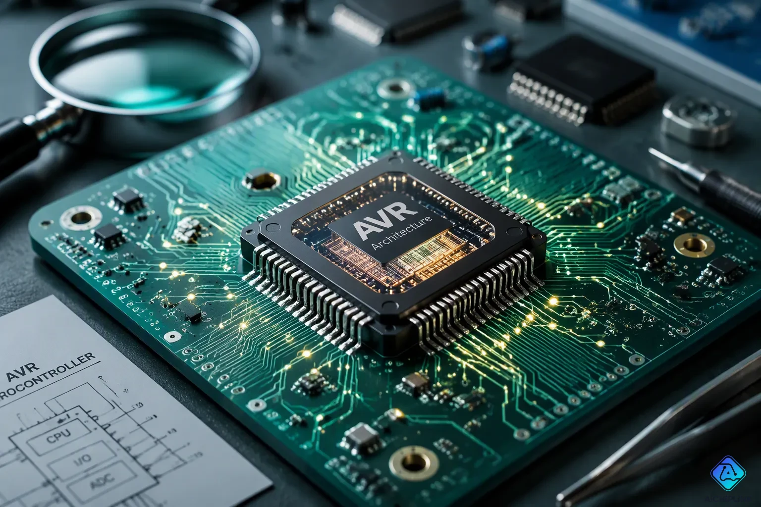
Think about your washing machine. It runs one set cycle, not a thousand apps. That's a microcontroller: a small chip built to control a single job inside a larger system. A regular computer handles many tasks at once. A microcontroller focuses on just one.
You find these chips everywhere. The AVR Microcontroller, an 8-bit RISC family from Atmel (now Microchip Technology), powers DIY electronics, robotics, and industrial control. Ever wonder how your drone decides to hover or your thermostat reads the temperature? That's a microcontroller making choices.
This article explains the inner design of AVR microcontrollers. We'll look at the key features that make them a top pick for engineers and hobbyists. You'll see what goes on inside that tiny chip.
Key Takeaways
-
AVR microcontrollers use a modified Harvard design and RISC setup to run instructions quickly, often in just one clock cycle.
-
They have three kinds of memory: Flash for the program code, SRAM for short-term data, and EEPROM for saving data that stays even when power is off.
-
The CPU has 32 general-purpose registers and a strong ALU, which allows it to work quickly and efficiently.
-
In-system programmability lets you update the chip's firmware easily without taking it out of the circuit.
-
AVRs use little power and work with many voltages, so they are great for battery-powered projects.
AVR Microcontroller Architecture Overview
Picture the inside of an AVR Microcontroller as a small city. The CPU acts as the city center, making all decisions. Memory blocks store different kinds of information. I/O peripherals serve as the city gates, connecting to the outside world. A bus system, like roads, links everything together. This simple layout powers millions of embedded devices.
Core Components: CPU, Memory, and I/O
The CPU, or central processing unit, executes instructions. It performs math, moves data, and controls the flow of operations. Think of it as the brain of the chip.
Memory comes in three forms. Flash memory stores your program code permanently. SRAM holds temporary variables while the chip runs. EEPROM saves data that must survive power loss. Each memory type serves a distinct purpose.
I/O peripherals handle communication. These include timers, analog-to-digital converters, and serial interfaces. They let the chip sense the world and respond. For example, the ATmega2560, a popular AVR chip, offers 54 digital I/O pins and 16 analog input pins. That gives you 70 total pins for connecting sensors, LEDs, motors, and other components. You can build complex projects without adding extra chips.
The Modified Harvard Architecture and RISC Design
The AVR Microcontroller uses a modified Harvard architecture. This design separates program memory from data memory. Program code lives in Flash memory. Data lives in SRAM and EEPROM. Each memory system has its own dedicated bus.
Why does this matter? Separate buses allow simultaneous access. The CPU can fetch an instruction from Flash while reading data from SRAM at the same time. This parallel operation speeds up processing considerably. The program bus is 16 bits wide for fetching instructions. The data bus is 8 bits wide for moving data. This combination works well for 8-bit microcontrollers.
The modified part of the architecture adds flexibility. A special instruction called LPM (Load Program Memory) lets you read constant data from Flash. This feature bridges the gap between program and data memory. You can store lookup tables or fixed strings in Flash and access them when needed.
The RISC philosophy complements this hardware design. RISC stands for Reduced Instruction Set Computer. The AVR uses a small, highly optimized set of instructions. Each instruction is 16 bits long and fixed in length. The CPU has 32 general-purpose registers, each 8 bits wide. Any register can work with any instruction, giving you great flexibility.
This design achieves remarkable efficiency. Most instructions execute in a single clock cycle. The two-stage pipeline fetches the next instruction while executing the current one. This means the chip processes up to 1 MIPS (million instructions per second) per MHz of clock speed. A 16 MHz AVR can handle roughly 16 million instructions each second.
Compare this to PIC microcontrollers. PIC chips use a different architecture that takes 4 clock cycles per instruction. The AVR's RISC design executes faster for most operations. This speed advantage makes AVRs ideal for real-time applications like motor control and signal processing.
The combination of Harvard architecture and RISC design creates a powerful yet simple system. You get fast execution, efficient memory use, and straightforward programming. These qualities explain why the AVR Microcontroller remains a favorite among engineers and hobbyists alike.
Memory Organization in AVR Microcontrollers
Memory in an AVR Microcontroller works like a neat filing system. Each memory type has its own job. Knowing these roles helps you write better code and build reliable systems.
Flash Memory: Storing the Program Code
Flash memory stores your program instructions. It is non-volatile, so it keeps data even without power. You can unplug your device, wait a week, and the program stays safe.
The AVR family was one of the first to use on-chip flash memory. This makes reprogramming easy. You do not need special tools or UV light erasers like older chips. Just connect a programmer, upload new code, and the chip updates.
Flash memory does not last forever. Microchip's official docs say the flash in chips like the ATmega328P can handle at least 10,000 write/erase cycles. That means you can reprogram it ten thousand times before wear matters.
Real tests show even better results. One engineer tried an experiment with a Chinese clone Arduino Nano. This board uses an ATmega328P chip. He programmed it over 80,000 times. The chip still worked perfectly. That is eight times more than the rated limit.
For most projects, you will never hit these limits. You might update firmware a few dozen times during development. Once deployed, the program rarely changes. Flash endurance is not a problem for typical uses.
SRAM and EEPROM: Data Storage and Persistence
SRAM is your working memory. This volatile storage holds variables, temporary values, and the stack while the chip runs. When power goes away, SRAM loses everything.
EEPROM offers a different kind of storage. This non-volatile memory keeps data that must survive power cycles. You might save calibration values, user settings, or high scores here. EEPROM keeps this info when the device turns off.
The data memory space splits into three parts. General-purpose registers (GPRs) sit at the lowest addresses. These 32 registers feed the CPU directly. I/O registers come next, controlling peripherals like timers and serial ports. SRAM takes up the rest for your variables and stack.
Pick the right memory for each task. Use flash for constants and lookup tables. Use SRAM for active calculations. Use EEPROM for data that must persist. This plan makes the best use of your resources and keeps programs stable.
The CPU Core and Instruction Execution
The CPU core is the heart of every AVR Microcontroller. It processes instructions, moves data, and controls all operations. Two main parts make this possible: the register file and the Arithmetic Logic Unit (ALU).
General-Purpose Registers and the ALU
Your AVR chip contains 32 general-purpose working registers. These are named R0 through R31. Each register holds one byte. The CPU assigns each register a data memory address. R0 sits at 0x0000. R31 sits at 0x001F. These first 32 locations of the data space map directly to the register file.
This mapping matters. The X, Y, and Z pointer registers can index any register in the file. Registers R26 through R31 serve a dual purpose. They work as normal registers and also form three 16-bit address pointers. R27:R26 is the X pointer. R29:R28 is the Y pointer. R31:R30 is the Z pointer. These handle indirect addressing of the data space.
The pointer registers support three addressing modes. You can use a fixed displacement to access a specific offset. You can use automatic increment to load and then advance the pointer. You can use automatic decrement to move the pointer backward and then load.
LD R1, X   ; Load from address X
LD R1, X+  ; Load from X, then increment pointer
LD R1, -X  ; Decrement pointer, then load from new address
The ALU sits next to the register file. It performs all arithmetic and logic operations. The ALU can add, subtract, and compare values. It can perform AND, OR, XOR, and NOT operations. It handles bit functions like shifting and rotating bits. Some AVR models include a hardware multiplier for signed and unsigned multiplication. This multiplier supports fractional format. The ALU reads two register operands, computes the result, and writes it back to the destination register. All this happens in a single clock cycle.
The Fetch-Decode-Execute Cycle and Pipelining
Every instruction goes through three stages. The CPU fetches the instruction from Flash memory. It decodes the instruction to understand what to do. It executes the instruction using the ALU and registers. This is the fetch-decode-execute cycle.
The AVR speeds up this cycle with pipelining. The Harvard architecture separates program memory from data memory. This allows the CPU to fetch the next instruction from Flash while it executes the current one. The fast-access register file also helps. The ALU can read two operands, perform the computation, and write the result back. All this happens within one clock cycle. This parallel design is the key reason the AVR achieves single-cycle execution. The pipeline has two stages: fetch and execute.
This parallel fetch-and-execute pipeline drives directly from the CPU clock. There is no internal division. The result is up to 1 MIPS per MHz. A 16 MHz chip processes about 16 million instructions per second.
Pipelining has one limitation. When a conditional branch instruction reaches the execution stage, the CPU must predict the branch outcome. The AVR always predicts that the branch will not be taken. This is the simplest implementation. The program counter naturally points to the next sequential instruction. However, branches are taken about 80 percent of the time. This prediction is often wrong. When the prediction fails and the branch is taken, the pipeline must flush and rebuild from scratch. This incurs a branch penalty of exactly one clock cycle for the 2-stage pipeline architecture.
This penalty is small. Most instructions still execute in a single cycle. The pipeline refills quickly. You can write code to minimize branch penalties. The CPU core remains efficient and responsive.
Key Features of AVR Microcontrollers
The AVR Microcontroller family stands out for several practical reasons. You can update firmware without removing the chip from your circuit board. This ability, called in-system programmability, saves time during development and makes field updates easier.
In-System Programmability and Peripherals
In-System Programming (ISP) uses the SPI protocol, a 3-wire synchronous standard. Three dedicated lines handle the communication: SCK (serial clock), MISO (master-in slave-out), and MOSI (master-out slave-in). SCK keeps the data transfer in sync. MISO carries data from the chip to the programmer. MOSI sends data from the programmer to the chip. You connect these three pins to a programmer, upload new code, and you are done.
For debugging, some AVR chips support the debugWIRE interface. This single-wire protocol works on classic ATtiny series microcontrollers and smaller ATmega models, including the ATmega328. You can step through your code, inspect variables, and find bugs while the chip runs in your circuit.
Built-in peripherals reduce the need for external parts. The ATmega328P, for example, includes several communication interfaces:
| Communication Interface | Pins |
|---|---|
| USART | PD0 (RXD), PD1 (TXD) |
| SPI | PB3 (MOSI), PB4 (MISO), PB5 (SCK), PB2 (SS) |
| I2C (TWI) | PC4 (SDA), PC5 (SCL) |
These interfaces let you talk to sensors, displays, and other microcontrollers without adding extra chips. Timers, analog-to-digital converters, and PWM outputs round out the peripheral set.
Power Efficiency and Versatility
Power consumption matters for battery-powered projects. The ATmega328P offers several sleep modes to save energy:
| Power-Saving Mode | Typical Current Consumption (1.8V, 1MHz, 25°C) |
|---|---|
| Idle | 40 µA |
| Power Save | 0.70 µA |
| Power Down | 100 nA |
Idle mode shuts down parts of the device. Power Save keeps a 32 kHz crystal running for timekeeping. Power Down shuts down everything, including the clock source.
Comparing power usage with ARM Cortex-M0+ chips reveals an interesting trade-off. The ARM draws 50–100 µA/MHz in active mode, while the AVR draws about 200 µA/MHz. However, the AVR consumes roughly 0.1 µA in deep sleep at 1.8V, beating the ARM's sub-1 µA figure. The AVR also wakes up faster due to simpler wake-up sequences and smaller leakage currents.
The operating voltage range adds versatility. The ATmega328P runs from 1.8V to 5.5V. The datasheet specifies a safe minimum of 1.8V for clock frequencies below 4MHz. You must reduce the maximum clock frequency as voltage decreases. This flexibility lets you power your project from two AA batteries or a standard 5V USB supply.
The AVR Microcontroller uses a modified Harvard architecture and a RISC CPU. This design keeps program memory separate from data memory. It also lets it run one instruction per clock cycle using pipelining. You get Flash for your program, SRAM for working data, and EEPROM for saving things when power is off.
These features make AVR chips easy to use and fast. You can update the program without taking the chip out. That is why they are popular in schools and for making new products.
Now you know the basics. Next, learn about interrupts, timers, and ways to talk to other devices. Get a development board and start trying things out. Working with the board will help you learn faster than just reading.

Written by Jack Elliott from AIChipLink.
AIChipLink, one of the fastest-growing global independent electronic components distributors in the world, offers millions of products from thousands of manufacturers, and many of our in-stock parts is available to ship same day.
We mainly source and distribute integrated circuit (IC) products of brands such as Broadcom, Microchip, Texas Instruments, Infineon, NXP, Analog Devices, Qualcomm, Intel, etc., which are widely used in communication & network, telecom, industrial control, new energy and automotive electronics.
Empowered by AI, Linked to the Future. Get started on AIChipLink and submit your RFQ online today!
Frequently Asked Questions
What makes AVR different from other microcontrollers?
AVR uses a RISC design with a modified Harvard architecture. Most instructions run in one clock cycle. That means faster processing than many similar chips. Program and data memory are separate, so the chip can access both at once. You get up to 1 MIPS per MHz of clock speed.
How do I choose the right AVR for my project?
First, count how many I/O pins you need. Then figure out how much memory you'll use. The ATtiny series works well for small projects with few pins. The ATmega series gives you more pins, memory, and peripherals. Before you decide, check the datasheet for timers, ADC channels, and communication options.
Is AVR still worth learning today?
Yes. AVR is still common in schools and industry. Its architecture teaches basic embedded concepts in a clear way. Arduino boards use AVR chips, so you get tons of tutorials and libraries. Many products still use AVR microcontrollers because they are reliable, cheap, and simple to program.
What is the practical difference between Flash, SRAM, and EEPROM?
Flash stores your program code permanently. SRAM holds temporary variables while the chip runs. EEPROM saves data that must survive power loss. Use Flash for instructions, SRAM for active calculations, and EEPROM for calibration values or user settings that need to persist.
How do I start programming an AVR microcontroller?
Get an Arduino board or a standalone AVR chip with a programmer. Install the Arduino IDE or Atmel Studio. Write your code in C or C++. Connect the programmer to the SPI pins. Upload your firmware. Start with blinking an LED, then move to sensors and communication protocols.