Build a SEPIC Converter with XL6009 A Practical Guide
You can set up the XL6009 as a SEPIC converter. This setup lets the output be higher, lower, or the same as the input voltage. The polarity also stays non-inverted. That flexibility makes the SEPIC a great choice for battery-powered designs. In these designs, the supply often drifts across the output level. The XL6009 is a versatile dc-dc converter IC, and this build shows one practical way to use it.
Good SEPIC Converter Design starts with part values. You will pick the inductors, capacitor, and diode, then lay out the PCB. By the end, you will have a built and tested board. It will have a checked voltage range and a measured efficiency figure.
Key Takeaways
-
A SEPIC converter keeps the output voltage steady even when the input voltage goes above, below, or equals it.
-
Choose the right inductors, capacitor, and diode first so your SEPIC converter works well.
-
Use two resistors, called a feedback divider, to set the output voltage.
-
Keep the high-current loop small on the PCB to lower noise and ripple.
-
Check your board safely with a power supply that limits current, and measure efficiency at different loads.
How the SEPIC Converter Works
Single-Ended Primary-Inductor Converter Basics
The SEPIC converter works through one switching cycle that has two phases. You can follow the energy flow in three steps:
-
Switch ON (closed): both inductors (L1 and L2) take in and store energy, while the output capacitor powers the load.
-
Switch OFF (open): the energy stored in both inductors is released and sent through the AC coupling capacitor to the load.
-
Over one full switching cycle, the average voltage-time product across each inductor adds up to zero, which keeps the circuit running steady.
The power stage of this single-ended primary-inductor converter has two inductors, an AC coupling capacitor (CAC), an output capacitor (Cout), a control transistor (Q1), and a diode or synchronous switch (Q2/D1). The coupling capacitor blocks DC transfer but still lets AC energy pass through. It also gives built-in output short-circuit protection.
When the switch is on, the input voltage Vin is applied directly across the coupling capacitor Cc, and its voltage stays fixed (not allowed to change) when the inductors are tightly coupled.
Component Roles and Non-Inverted Output
The single-ended primary inductor converter keeps its output polarity the same as the input. Energy moves through the coupling capacitor, not through a transformer winding, so no inversion happens. That is why the output voltage can be higher or lower than the input voltage, or match it exactly. So one board can step the input voltage up or down as the battery drains.
The XL6009 is a dc-dc converter that you can set up as a boost, flyback, SEPIC, or inverting converter. You pick the SEPIC here because it handles a drifting supply without flipping polarity. A boost converter IC based SEPIC buck-boost converter design like this one covers the full battery range. Even a simplified SEPIC converter keeps that advantage. The two inductors and one coupling capacitor make up the core of the circuit.
SEPIC Converter Design with the XL6009
Inductors, Coupling Capacitor, and Diode
A good SEPIC converter design begins with choosing the right part values. You figure out the two inductors, the coupling capacitor, and the Schottky diode from four inputs: input voltage, output voltage, load current, and switching frequency. The table below shows the sizing rules for the inductors.
| Parameter | Sizing Guideline | Rationale |
|---|---|---|
| Inductance (per winding) | 6.8 µH per winding (example design) | Set by the design calculation for your operating point |
| Rated current | Above maximum input current in boost mode, with margin | Rated per winding (1:1 ratio); use more margin than a buck needs |
| Saturation current | Above maximum peak inductor current (average plus half the AC ripple) | Rated per winding; margin guards the peak |
| Average inductor current | Top winding carries the input current | Input current flows in one winding, output current in the other |
The SEPIC coupling capacitor carries high AC current, so it needs very low ESR. You usually get that by putting several MLCCs in parallel. Its voltage rating must be higher than the maximum input voltage plus ripple, because the capacitor charges to the input voltage when the primary switch is on. Its RMS current rating grows with output power, since all output current passes through it. Pick the output diode for low forward drop; Schottky losses pull efficiency down at higher output currents.
A coupled inductor is a valid alternative to two separate inductors. A dual-winding part on one core cuts component count and board space. Close coupling splits the ripple between windings, so you need only about half the inductance for the same ripple amplitude. Coupling also steers ripple from the input winding to the output winding, which lowers conducted EMI. Separate inductors fit best when you want simple sourcing or wide spacing. A coupled part suits compact boards, and higher leakage inductance can actually help here.
Feedback Divider and Output Setting
The XL6009 has no directly variable output. A feedback circuit sets the output voltage instead. The controller IC compares the divided output against its internal reference and adjusts switching to hold regulation. You choose two resistors, R1 from output to the feedback pin and R2 from that pin to ground. The output voltage equals the reference voltage times one plus R1 divided by R2. Pick R2 in the low tens of kilohms to keep the divider current small, then solve for R1. Check the reference value in the XL6009 datasheet before you calculate.
This dc-dc converter serves portable electronic equipment, so its current limits matter. Keep your load within the switch current rating across the whole input voltage range. A wider input voltage range raises the peak switch current in boost mode, so verify the worst case. The output capacitor and output diode then handle the pulsing energy the SEPIC delivers. Follow these SEPIC converter design steps, and your SEPIC converter design will hold up on the bench. Careful SEPIC converter design pays off at every load point.
Schematic Diagram and PCB Layout
Reading the Complete Schematic
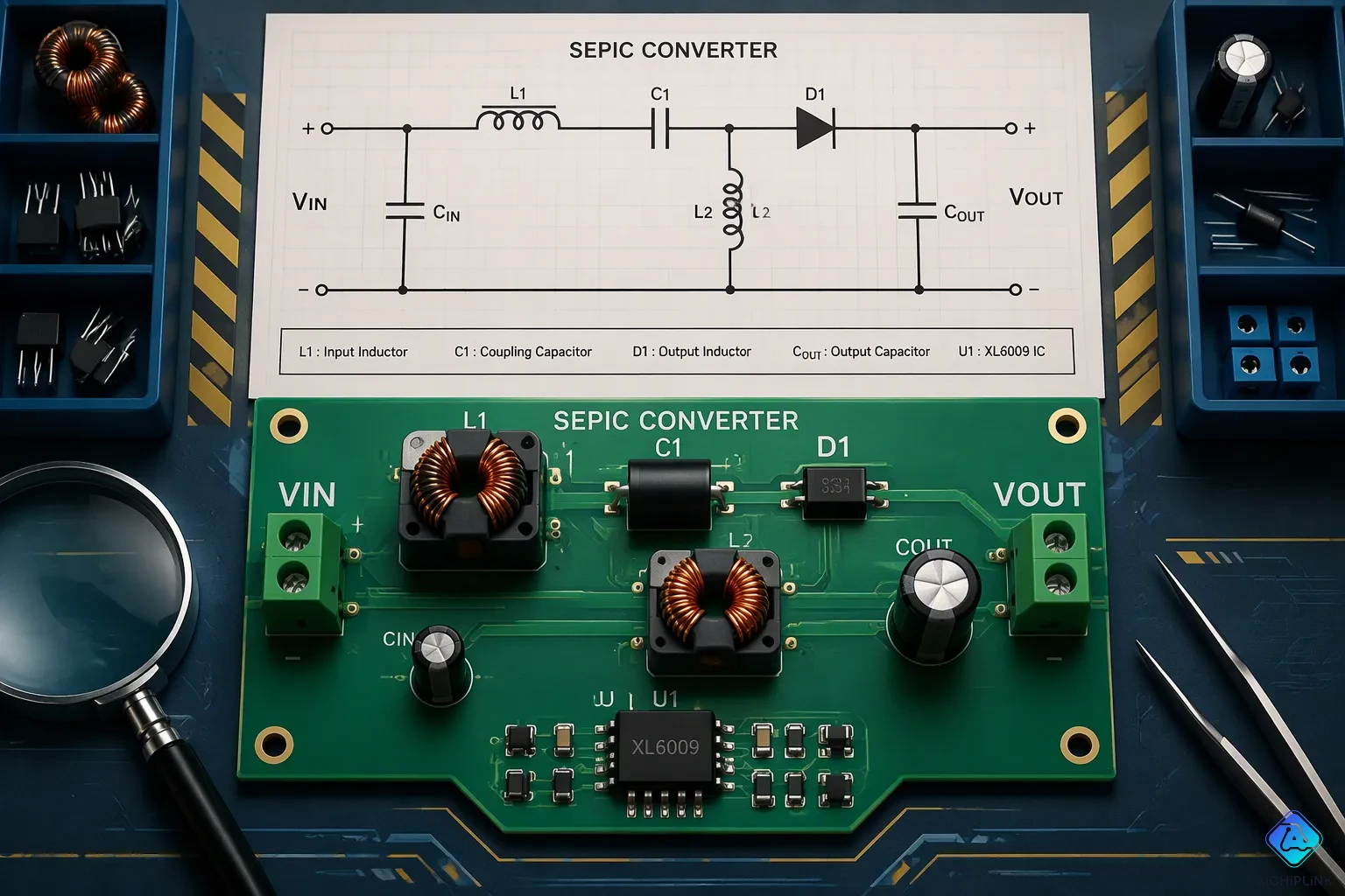
The schematic diagram shows a short, easy-to-follow signal path. Start at the input terminal. The input voltage goes to L1 and the input capacitor. L1 connects to the switch node, and the XL6009 switch pin drives that node. L2 sits between the coupling capacitor and ground, so both inductors share the same switch node on one side. The coupling capacitor links the switch node to the diode anode. The diode cathode feeds the output capacitor and the output terminal. The feedback divider taps the output voltage and sends it back to the feedback pin. Read the schematic diagram in that order, and every connection has a clear purpose.
Layout Tips and Layout Priorities
The SEPIC topology is basically a non-inverting buck-boost converter that can step a DC voltage up or down, and it has two switching voltage nodes and one switching current loop.
That single switching current loop sets your layout priorities. In a SEPIC converter, the high-frequency current loop is made by the two switching devices and the two capacitors. The inductor current cannot change instantly, so it limits di/dt. The current magnitude is fixed by the output power you need, so the main layout approach is to make the physical loop area as small as possible. This suppresses the near-field magnetic field from this noise source. Capacitor placement matters most: mounting the capacitor on the back side of the device shortens the distance to the switching devices. This measurably lowers noise compared with placing it beside the device or using long leads.
Apply these priorities to your design:
-
Reduce the high di/dt loop area first; the critical noisy loops include the MOSFET switch loop, diode loop, coupling-capacitor loop, output-capacitor charging loop, and gate-drive loop.
-
Cluster the MOSFET, diode, coupling capacitor, and output capacitor tightly together to shrink loop areas.
-
Keep the switch-node copper small and never route sensitive feedback traces near it.
-
Place the coupling capacitor close to the MOSFET, diode, and inductors, and avoid pushing coupling-capacitor current through long traces.
-
Use a solid ground plane and connect power ground and signal ground carefully.
-
Place the feedback divider close to the controller feedback pin and use Kelvin sensing for output feedback when needed.
-
Keep the gate-drive trace short, use wide copper for high-current paths, and keep the input capacitor close to the input inductor and switch path.
The board files are ready to download as a Gerber package. Import the Gerber file into your fab house's viewer and check the copper layers, silkscreen, and drill file before you order. A quick visual check of the schematic against the layout catches most first-run mistakes.
Testing the SEPIC Converter
Safe Power-Up Procedure
Bench testing carries real risk, so set up your supply with care. Use a current-limited bench supply and set the limit below the expected input current. This step protects the board from a wiring mistake. Check the polarity of every connection before you apply power. A reversed input can destroy the XL6009 and the diode in an instant.
Never apply full power to an untested board. Start with no load, then add load in steps.
Begin with no load at first power-up. Watch the input current on the supply meter. A sudden jump means a short or a wrong part. Measure the output voltage at the output terminal and confirm it sits near your target. Add a small load and check that regulation holds. Then raise the load in steps and log the output current at each point. Write every reading in a notebook so you can compare runs later.
Expected Voltage Range and Efficiency
A working SEPIC converter delivers a stable output across the full input span. Set the input voltage above the target output and confirm the board bucks down. Set the supply below the target and confirm it boosts up. Set the supply equal to the target and confirm the output stays in regulation. This three-point check proves the output voltage range you designed for.
Efficiency varies with load, so measure it at several points. Record input power and output power at light, medium, and full load. Divide output power by input power to get efficiency at each point. Expect the best figure near the middle of the load range. Light loads lose ground to switching losses, and heavy loads lose ground to conduction losses. Compare your numbers against the design target and note any gap. A well-built SEPIC should hold close to its target across the range. Repeat the sweep after any part change.
Improving SEPIC Performance
Reducing Ripple and Noise
You can lower output ripple by picking better capacitors. Use low-ESR parts and put several of them side by side. The output capacitor handles pulsed current, so ESR causes most of the ripple voltage. Add a small ceramic cap near the load to catch high-frequency spikes. A snubber across the diode or switch calms ringing at the switch node. Choose snubber values on the bench, then look at the waveform again.
Layout changes finish the job. Make the high-current loop area smaller and keep the switch node copper small. Route the feedback trace away from the switch node. These steps cut both ripple and radiated noise.
Extending Input Range and Protection
A cascading approach stretches the usable input voltage range. A small boost converter steps up a low input first. That boosted rail then powers the XL6009. This trick gives your wide-input-range dc-dc converter more headroom at the low end. The XL6009 keeps its own input voltage range, so check that the boosted rail stays inside it.
Protection upgrades keep the board alive. Add a fuse at the input to limit fault current. A reverse-polarity diode or MOSFET blocks a wrong connection. Give the switch and diode copper pours for thermal relief. These parts give off heat, and extra copper spreads it. A wide-input-range design gains the most, because the input voltage swings far and losses shift with it.
Test each change one at a time. Measure ripple and efficiency after every tweak. This SEPIC converter rewards careful tuning, and your wide input voltage range ability grows with each fix. A well-protected SEPIC handles rough bench conditions and still delivers a stable output voltage.
You began with the switching cycle and saw how energy moves through the two inductors and the coupling capacitor. Then you picked the parts, set the feedback divider, read the schematic, and laid out the board. Your bench tests showed the output stays on target above, below, and equal to the input. You now have a checked SEPIC converter design with a measured efficiency number.
Your next steps are practical. Try low-ESR output capacitors, a snubber, or a tighter high-current loop to cut ripple. Add a fuse and reverse-polarity protection for rough bench conditions. Share your measured results, and compare them with other builders. Each run teaches you something new about this SEPIC.

Written by Jack Elliott from AIChipLink.
AIChipLink, one of the fastest-growing global independent electronic components distributors in the world, offers millions of products from thousands of manufacturers, and many of our in-stock parts is available to ship same day.
We mainly source and distribute integrated circuit (IC) products of brands such as Broadcom, Microchip, Texas Instruments, Infineon, NXP, Analog Devices, Qualcomm, Intel, etc., which are widely used in communication & network, telecom, industrial control, new energy and automotive electronics.
Empowered by AI, Linked to the Future. Get started on AIChipLink and submit your RFQ online today!
Frequently Asked Questions
Can the output sit above and below the input on the same board?
Yes. The SEPIC topology keeps the output non-inverted, so one board can step up, step down, or pass the input straight through. You set the target with the feedback divider, and the converter holds regulation as the supply drifts across that level.
Why use two inductors instead of one?
The two inductors store and release energy in alternating phases, and the coupling capacitor passes that energy to the output. A single inductor cannot do this job in a SEPIC converter. A dual-winding coupled inductor on one core is a valid substitute and saves board space.
How do I set the output voltage?
The XL6009 has no directly variable output. Two resistors form a divider from the output to the feedback pin. The output equals the reference voltage times one plus R1 divided by R2. Check the reference value in the datasheet, pick R2 in the low tens of kilohms, then solve for R1.
What causes high ripple, and how do I fix it?
Most ripple comes from the output capacitor's ESR, because that capacitor handles pulsed current. Use low-ESR parts and parallel several of them. Shrink the high-current loop area, keep switch-node copper small, and route the feedback trace away from the switch node.
Can I extend the input range below the XL6009's limit?
Yes. Add a small boost converter ahead of the board. It steps up a low input first, and that boosted rail then powers the XL6009. Check that the boosted rail stays inside the XL6009's own input range. Add a fuse and reverse-polarity protection for rough bench conditions.