Discrete FPGA and CPU vs SoC FPGA: Which is Better?
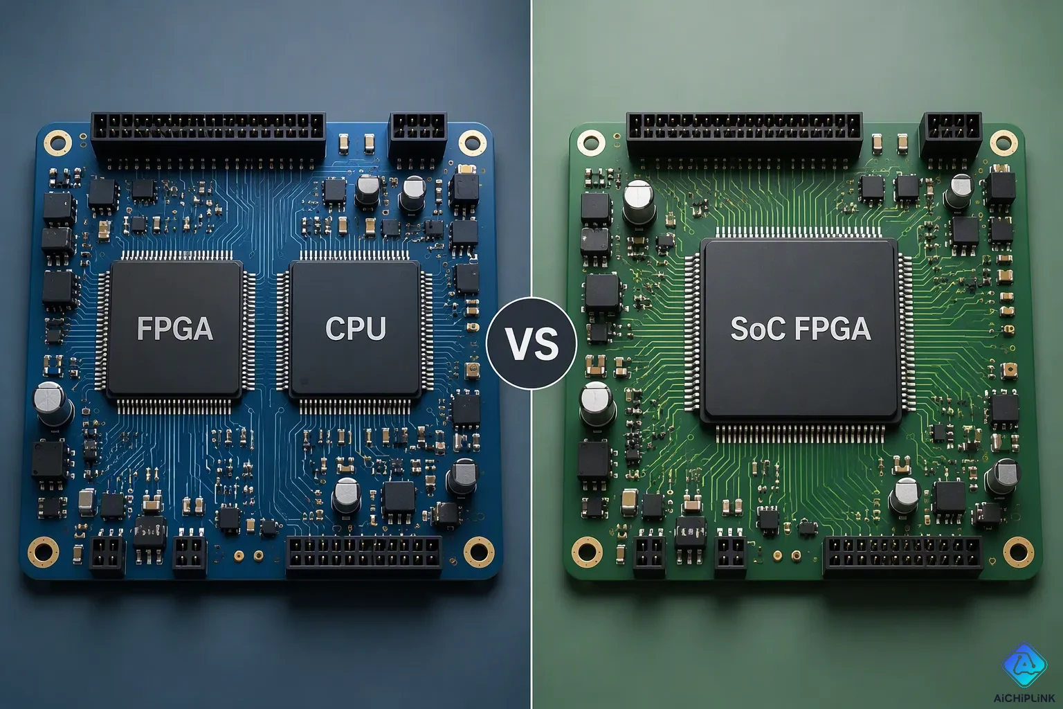
You sit at your workstation, cursor blinking over an empty schematic. Two paths stretch before you. Should you pair a separate FPGA with its own CPU, or pick an all-in-one SoC? The answer isn't about which tech wins everywhere—it's about what matters most for your specific needs. This is the classic FPGA vs SoC decision, and it goes far beyond a simple spec sheet comparison.
This article looks at the real trade-offs in the FPGA vs SoC debate. You'll see how each choice affects speed, power use, and flexibility. You'll find out which option fits different jobs, from small edge devices to big data centers. Each path changes how you plan your processor, and understanding the FPGA vs SoC distinction early on can save you months of rework down the line.
The choice between FPGA vs SoC shapes your whole project—from how you handle parallel processing to how you manage software updates. Knowing these differences helps you pick wisely, whether you're prototyping a custom accelerator or building a production-ready system. Let's check out both paths together and see which one aligns with your goals.
Key Takeaways
-
SoC FPGAs save power and space by putting the processor and FPGA together on a single chip.
-
Discrete FPGA and CPU setups let you upgrade each part on its own.
-
SoC FPGAs make board design easier and cut down on the extra parts you need.
-
Discrete setups let you pick the best processor and FPGA from different vendors, giving you more flexibility.
-
Your choice depends on what your application needs for power, speed, and the ability to upgrade later.
FPGA vs SoC: Defining the Two Approaches
The FPGA vs SoC debate is about design philosophy. Each approach serves different priorities. Your choice depends on how you value modularity versus integration. One path gives you separate components you can upgrade independently. The other path gives you a single chip with everything built in. Both paths have their strengths and weaknesses. Understanding these differences helps you choose the right path for your next project.
Discrete FPGA + Processor: A Modular Pair
A discrete setup connects a standalone FPGA to a separate processor. These chips communicate through high-speed interfaces. You connect them with a printed circuit board that routes signals between the two devices. The connection uses standard protocols that many designers already know.
The PCIe implementation uses a PIPE interface. This enables high-speed communication across Gen3, Gen5, and Gen6 links. Ethernet like 100GbE serves as another key interface. These interfaces give you the bandwidth you need for demanding tasks like video processing or data acceleration.
Real-world examples show this approach. AWS EC2 F1 instances pair Xilinx Virtex UltraScale+ FPGAs with Intel Xeon CPUs. This setup gives you eight virtual cores alongside reconfigurable hardware. The Intel Agilex FPGA also connects with Intel Xeon processors through Compute Express Link. This cache-coherent link offers low latency and tight connectivity.
The discrete FPGA + processor model gives you independent upgrade paths. This suits applications where performance requirements evolve. You can replace the central unit without changing the logic array. You can also upgrade the logic array without replacing the central unit.
System-on-Chip: Integrated FPGA and CPU
A system on chip merges hard processor cores and field-programmable gate arrays fabric. This creates a tightly coupled soc architecture. The soc design reduces board complexity. You save space on your printed circuit board. You also lower power consumption because data moves between the two parts without leaving the chip. The integrated nature makes the system-on-chip ideal for many applications.
The FPGA architecture in a discrete setup differs from the integrated approach. The integrated path gives you tighter integration. The FPGA vs SoC decision here becomes a trade-off. The integrated approach works well for embedded applications. You can write software and hardware logic within the same toolchain. This simplifies your development workflow. You spend less time on debugging and testing.
Performance and Power Trade-offs
Often, how fast your system works and how much power it uses will decide which path you choose. The fpga vs soc comparison makes the most sense when you look at how each method handles real jobs. You need to know these differences before you pick a design. The right choice depends on the tasks your system must do and where it works.
Throughput and Latency
Field-programmable gate arrays are very good at doing many tasks at the same time. You can handle thousands of data streams at once. This makes them great for jobs that need to finish by a set time, like live video processing or fast trading. Each logic block works on its own, so you get a lot of work done without waiting for one step after another.
A CPU, on the other hand, is better at tasks that go step by step. Processors run at much faster clock speeds, often several gigahertz. This speed helps when your work follows a clear order. The processor does one instruction after another, but it does them very fast. For jobs like running an operating system or making complex choices, the CPU beats the FPGA.
The fpga performance is best for pipelines that move a lot of data. You can build custom accelerators that handle data as it comes in. There is no need to wait for a bus cycle or a scheduler. The soc performance combines that parallel power with a processor's step-by-step strength. You get both types of power on one chip.
Latency is another important factor. A separate FPGA and CPU must talk through outside connections. Signals move across the board, which adds a few nanoseconds of delay. An SoC keeps the processor and programmable logic on the same chip. Data moves through inside paths, cutting down latency a lot. For tasks that need fast response, this difference is important.
Think about a motor control loop. The system must read sensor data, figure out the fix, and send the output in microseconds. An SoC FPGA does this with very little delay. A separate setup adds overhead from the interface, which could go over your time limit.
Power Efficiency and Management
How well your system uses power often decides which method fits your project. SoC FPGAs usually use less power for the same amount of work. The built-in design removes outside drivers and cuts down on signal changes across board traces. Every little bit of power you save on the interface goes to useful work.
Modern separate FPGAs have power-saving features. You can turn off unused logic blocks and change voltage levels as needed. These features make the two methods closer in power use. But the separate solution still needs power for two different chips. Each chip needs its own voltage regulators, clock sources, and capacitors. These extra parts add to your total power use.
SoCs have more advanced ways to manage power as it changes. The processor can control the power state of the programmable logic. You can turn off the FPGA fabric when not in use and wake it up when needed. This fine control works well for battery-powered devices where every millisecond matters.
The balance between performance and power efficiency depends on your work. A separate FPGA with a low-power processor might be as efficient as an SoC for some tasks. But the SoC makes your power setup simpler. You manage one device instead of handling two separate power areas.
Your choice also changes how you manage heat. A single SoC package puts all the heat in one spot. You might need a bigger heatsink or a fan. A separate setup spreads heat across the board, which could make cooling easier. Each method has its own challenges for your system's overall efficiency.
The jobs you want to do will guide your choice. Small edge devices that need long battery life often pick SoC FPGAs. Big computing systems with lots of cooling might choose separate parts. Knowing these trade-offs helps you pick the design that meets your performance and power needs.
Flexibility and System Complexity
Scalability and Upgradability
A discrete FPGA + processor setup lets you upgrade parts on their own. You can swap the processor without touching the FPGA fabric. You can also replace the FPGA when you need more logic space. This modular design works well when needs change over time. You might start with a basic processor and upgrade later. Or you might keep the same CPU while growing your programmable logic. This flexibility helps teams that expect changing workloads.
An SoC locks both parts into one package. You cannot upgrade the processor separately from the programmable logic. The SoC design fixes your setup from day one. If you need a faster processor, you must rebuild the whole board around a new chip. This limit matters for products that last a long time. You must guess your needs years ahead. Many teams find this okay for embedded uses with steady needs.
The discrete path also lets you pick the best parts from different makers. You can pair a special processor with an FPGA from another vendor. This freedom gives you more control over how your system performs. You can tune each part for its own job. The integrated approach forces you to accept the vendor's chosen balance. That trade-off affects your flexibility in ways you might not see until late in development.
Board Design and Footprint
Board complexity differs a lot between the two approaches. A discrete FPGA + processor needs careful routing of high-speed links. You need PCIe traces, clock distribution networks, and termination parts. Each connection adds design risk and layout work. You also need separate power areas for each chip. This increases your printed circuit board layers and total size.
A system-on-chip makes your board much simpler. The processor and programmable logic share one package. Data moves through internal paths instead of outside traces. You remove many interface parts completely. You need fewer decoupling capacitors and clock generators. This reduction shrinks your footprint a lot. Space-limited applications benefit greatly from this integration.
The SoC design also lowers your power distribution complexity. You manage one device instead of coordinating two separate power trees. This simplification shortens your design time. You spend less time on signal integrity analysis and more time on your actual logic. For portable devices and edge applications, this benefit often outweighs other factors. Your final product becomes smaller, lighter, and easier to build reliably. That practical flexibility helps your production team as much as your design team.
Cost Considerations
Money often decides the FPGA vs SoC question before you even look at technical specs. You need to look past the price tag of each chip. The real cost includes every resistor, connector, and engineering hour that goes into your product. Knowing these numbers early helps you avoid budget surprises later.
Bill of Materials and Unit Cost
A discrete FPGA + processor setup often shows a lower price per chip on paper. You can shop around for each part. You might find a cheap processor from one vendor and a budget FPGA from another. This approach gives you buying flexibility that a fixed package cannot match.
But your bill of materials tells a fuller story. Each separate chip needs its own support parts. You need voltage regulators for two power areas. You need clock generators for each device. You need level shifters and termination resistors for every high-speed link. These small parts add up quickly across thousands of units.
An SoC puts the processor and programmable logic in one package. You remove many extra parts entirely. Your board needs fewer capacitors, fewer oscillators, and fewer connectors. Your assembly cost drops because you place fewer parts. Your inventory management becomes simpler with one main chip to track.
The unit cost comparison depends on how many you make. Low-volume projects might like the discrete approach with cheaper individual parts. High-volume products often benefit from the SoC's lower system cost. You must calculate your total cost per board, not just the cost per chip.
Engineering Effort and Time-to-Market
Your development time is a hidden cost that many teams overlook. A discrete FPGA + processor requires you to design and test the link between two chips. You must write drivers for the PCIe or Ethernet interface. You must handle protocol handshaking and data alignment. This integration work takes weeks of engineering effort.
An SoC lets your software team start writing firmware while your hardware team sets up the programmable logic. Both groups work in the same toolchain. They share memory space and debug tools. This parallel workflow shortens your development schedule a lot.
The SoC approach also makes your board testing simpler. You power one device instead of handling two separate power sequences. You debug one clock domain instead of syncing multiple references. Your team spends less time on low-level setup and more time on your actual applications. This efficiency directly affects your time-to-market and your engineering budget.
Your choice also affects your long-term maintenance costs. A discrete setup lets you swap one part when it goes end-of-life. An SoC forces a complete redesign when the vendor stops making the chip. Think about your product's expected lifespan when weighing these options. The cheapest path today might cost more over your product's full life.
Development Workflow and Tools
Your development workflow shapes how quickly you move from concept to working product. The tools you choose affect every stage of your project. SoC FPGAs offer a unified path that lets hardware and software teams work together from day one. Discrete setups demand more coordination between separate toolchains and teams.
Hardware-Software Co-Design
SoC FPGAs run operating systems directly on their embedded processors. This capability transforms your development process. Software engineers write C/C++ code for the Arm cores while hardware designers configure the programmable logic in parallel. Both teams share the same design environment, which removes many handoff delays.
The AMD Vitis unified software platform demonstrates this integrated approach. You work in a single environment that targets FPGA fabric, Arm processors, and AI Engines together. The platform sits alongside the Vivado Design Suite, giving you a higher level of abstraction. Vitis Embedded supports C/C++ application development for the Arm subsystem. Vitis HLS lets you synthesize C/C++ functions into hardware logic without writing RTL manually.
The platform includes an open-source runtime library that manages data movement between computing domains. You also access over 400 pre-optimized libraries across eight categories, including DSP, Vision, and AI. These libraries accelerate common tasks with minimal code changes. For AI developers, the Vitis AI layer integrates with standard frameworks like TensorFlow and PyTorch.
A discrete FPGA and separate processor require you to bridge two distinct development ecosystems. You write firmware for the processor in one toolchain. You develop hardware logic in another. Then you must create custom communication protocols between them. This integration work consumes weeks of engineering time that an SoC approach avoids entirely.
Debugging and Testing
Debugging an SoC FPGA differs significantly from troubleshooting a discrete pair. The integrated chip offers on-chip tracing and shared memory between processor and programmable logic. You can observe both domains from a single debug session. This visibility speeds up your testing cycles considerably.
Vitis heterogeneous simulation provides unified simulation of AI Engine and programmable logic. You can validate hardware-in-the-loop using existing testbenches from MATLAB or Python. This feature lets you verify your complete system before committing to physical hardware.
A discrete setup forces you to use external logic analyzers for cross-domain debugging. You must synchronize multiple clock domains and trace signals across board traces. Each interface adds another layer of complexity to your testing process. You spend valuable time isolating whether a bug lives in the processor code, the FPGA logic, or the communication link between them.
The SoC approach gives you better visibility into your entire system. You can trace a data packet from the processor through the programmable logic and back again without leaving your development environment. This unified view reduces debugging time and helps you ship reliable products faster. For complex applications requiring tight hardware-software interaction, this advantage proves decisive.
Real-World Use Cases
Real projects show you which path works best. The FPGA vs SoC choice becomes clearer when you look at real uses. Each method serves different jobs with different needs. Your choice depends on matching the right tool to your specific work.
When Discrete FPGA + CPU Wins
High-performance computing often picks the discrete setup. You pair a special processor with a big FPGA to handle many parallel tasks. The FPGA + processor combo works best when you need the most computing power. Data centers use this setup for jobs like search ranking and video transcoding.
Custom networking gear also benefits from this modular design. You can use a standalone FPGA that processes packets at full speed. Your separate processor handles control tasks. This split lets you upgrade each part on its own. Network speeds change faster than control software. You can swap the FPGA for a newer model without changing your processor board.
Think about the AWS EC2 F1 instance model. You get Xilinx UltraScale+ FPGAs paired with Intel Xeon CPUs. This setup gives you eight virtual cores plus reconfigurable hardware. Developers use this for financial modeling and genome sequencing. The FPGA + CPU approach lets you scale compute power separately from logic resources.
Another example involves special processors. Some jobs need unique CPU features like vector extensions or specific security enclaves. You might pick a rare processor that has no integrated FPGA version. The discrete path gives you that freedom. You choose the best processor for your step-by-step tasks. You pick the best FPGA for your parallel tasks. This flexibility matters when your performance needs require specific hardware features.
When SoC FPGA is the Better Fit
Edge AI tasks often pick the integrated route. You use a system-on-chip that combines Arm cores with programmable logic. This SoC handles inference directly at the sensor. You avoid sending data to the cloud. The tight link cuts down latency and improves privacy. Power efficiency matters a lot in battery-powered devices. The SoC design saves energy by keeping data movement inside the chip.
Motor control systems also benefit from this integration. You need real-time response to sensor inputs. The processor runs the control algorithm while the FPGA handles PWM generation. Data moves between them through internal buses. This setup gives you the performance you need for precise motion control. The Xilinx Zynq family shows this approach. Its hardened processor cores work alongside programmable logic on one chip.
Portable medical devices are another strong use case. You need small size and low power use. The system-on-chip shrinks your board size a lot. You remove separate clock generators and interface parts. Your device becomes lighter and more reliable. The integrated design makes power management simpler. You control both parts from a single power tree.
The Intel Agilex series shows how SoC platforms handle tough edge tasks. You get advanced AI acceleration plus general-purpose processing. This combo works well for industrial inspection and self-driving vehicles. Your performance and power efficiency improve because you remove external communication overhead.
Think about your deployment environment carefully. Remote sensors and handheld tools benefit from SoC integration. The fewer parts improve reliability in harsh conditions. You have fewer solder joints that might break. Your system becomes easier to certify for medical or auto use. These tasks need predictable behavior and long life.
The choice finally depends on your product's priorities. High-end computing systems with good cooling often pick discrete parts. Small devices with strict power budgets choose integrated solutions. Your performance needs guide this decision. Your team's skills matter too. Some engineers are good at board-level integration. Others like working in one toolchain. Match your approach to your strengths and your application's real needs.
The better choice depends on your application. SoC FPGAs provide tight integration and better power efficiency for embedded designs. Discrete FPGA and CPU setups give you greater flexibility for independent upgrades and peak performance characteristics. Ask yourself: Does power efficiency matter for your application? Do you need to upgrade components independently? Explore hybrid approaches or specific product families like AMD/Xilinx Zynq and Intel Stratix 10. The performance characteristics of these devices suit different applications. Both paths are viable. A well-informed choice leads to success.

Written by Jack Elliott from AIChipLink.
AIChipLink, one of the fastest-growing global independent electronic components distributors in the world, offers millions of products from thousands of manufacturers, and many of our in-stock parts is available to ship same day.
We mainly source and distribute integrated circuit (IC) products of brands such as Broadcom, Microchip, Texas Instruments, Infineon, NXP, Analog Devices, Qualcomm, Intel, etc., which are widely used in communication & network, telecom, industrial control, new energy and automotive electronics.
Empowered by AI, Linked to the Future. Get started on AIChipLink and submit your RFQ online today!
Frequently Asked Questions
What applications work best with discrete FPGA and CPU?
You use this setup for high-performance computing, custom networking, and data center tasks. These applications need to upgrade parts on their own and get the most computing power. The FPGA handles many tasks at the same time for you.
What applications suit SoC FPGAs better?
You pick an SoC FPGA for edge AI tasks, motor control, and portable medical devices. These applications need small size, low power, and a close connection between parts.
How do your applications guide the choice?
Your applications tell you which way to go. You pick SoC integration for real-time control. You choose discrete parts for fast data processing. Fit your method to what your application needs.
Can you use a hybrid approach for complex applications?
Yes, you can combine both. You pair an SoC with an outside processor for extra power. This hybrid approach works for applications with different performance needs.
What about making your applications ready for the future?
You can upgrade discrete parts on their own. With SoCs, you must build a new board. Plan for how your applications will change over time. Fit future applications to the method you pick.