How to Design High-Side Switching Circuits with P-Channel MOSFETs for 2026
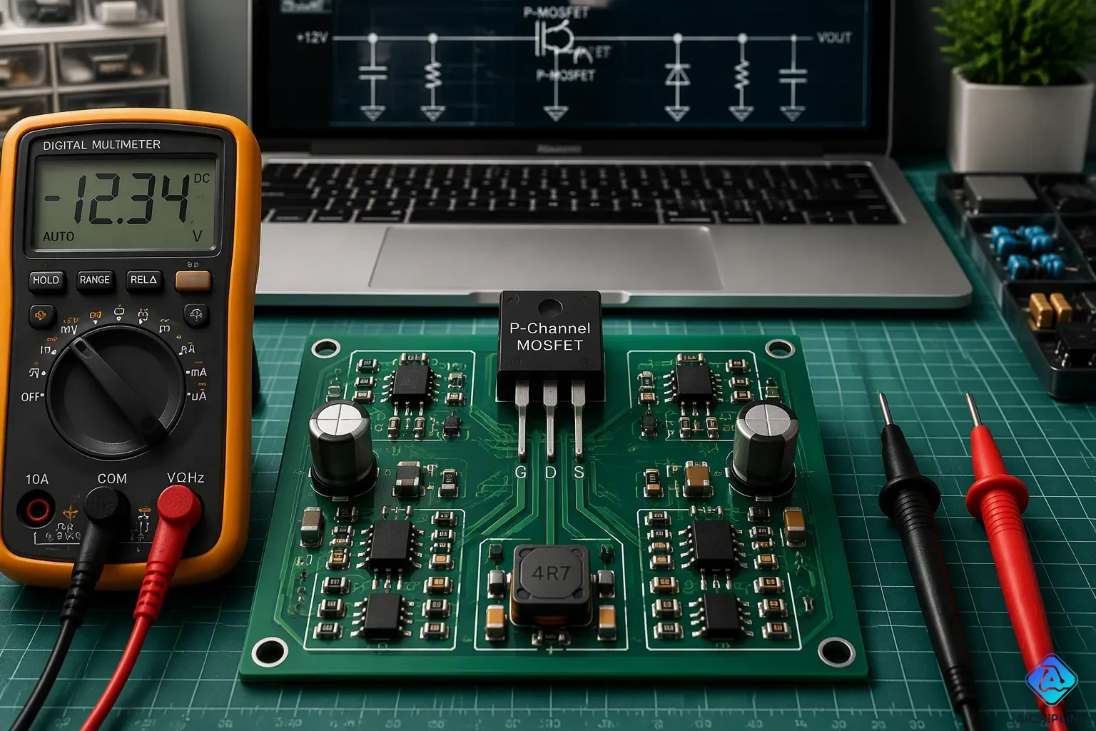
To switch power to a load that shares ground with your microcontroller, you need a method that keeps that ground intact. Low-side switching would break the shared ground, so the answer is high-side switching, which controls the positive power line. This approach preserves your ground connection and ensures stable operation.
P-channel MOSFETs offer a straightforward path to design reliable high-side switching circuits. Their gate control is intuitive: the device turns off when the gate voltage equals the source voltage. This guide walks you through the essentials—selecting the right components, crafting a safe gate drive, and adding critical protections. Each step brings you closer to a robust high-side design that can handle real-world conditions. You’ll also learn how to shield your circuit from voltage spikes, reverse currents, and other practical challenges. With this knowledge, you can transform a basic p-channel setup into dependable, field-ready hardware. Let’s get started on building your switching circuit.
Key Takeaways
-
Pick a P-channel MOSFET whose voltage and current limits are at least 1.5 times what your power source and load require.
-
Use an NPN transistor level shifter for gate control. A voltage divider causes slow switching and overheating.
-
Place a flyback diode across inductive loads to stop voltage spikes from harming the MOSFET.
-
You can protect against too much voltage by putting a Zener diode between the drain and source, and choose one with a voltage below the MOSFET's maximum rating.
-
Test your circuit with everything running at full power, and tune the gate resistors so the switch turns on and off quickly and cleanly, which keeps heat low.
Selecting the Right P-Channel MOSFET
Choosing the correct component forms the first step to design reliable high-side switching circuits. Get the datasheet numbers right, and you build on a solid foundation. Miss them, and you invite overheating or outright failure.
Key Parameters: Vds, Id, and Rds(on)
Three parameters carry the most weight when you design a high-side circuit. Drain-source voltage (Vds) defines the maximum voltage across the device. For a 12V supply, apply a safety margin. Industrial designs recommend 1.5 to 2 times the supply voltage to cover back-EMF spikes. That means a Vds rating of at least 24V. Continuous drain current (Id) must exceed your load current. A 5A load needs a part rated for more than 5A. Vgs_th sits between -2V and -4V. Vgs_max sits at ±20V. Stay within this limit. Many p-channel mosfets target these specifications.
| Parameter | Recommended Safety Margin |
|---|---|
| Drain-source breakdown voltage (Vds) | 1.5 to 2 times the supply voltage to provide margin for back-EMF spikes. |
| Continuous drain current (Id) | Must exceed both the motor's rated current and stall current, with additional margin based on thermal design. |
Rds(on) drives power loss and heat generation. Lower on-resistance means less heat for the same current. For a 5A load, target an Rds(on) under 0.1 ohms. The TO-220 package handles this power level well.
A TO-220 package in free air has a junction-to-ambient thermal resistance of about 50 °C/W. Each watt of dissipation raises the junction temperature by roughly 50°C above ambient.
A Practical Selection Example: 12V, 5A Load
This high-side switching example uses a common approach. Apply the selection rules to a real case. Your supply runs at 12V, and you need to switch 5A. Start with Vds. Apply the 1.5 to 2 times safety factor. That yields a minimum Vds of 18V to 24V. A -30V part gives comfortable margin and handles transients without stress. Next, set the current rating. Choose an Id that exceeds 5A by a healthy margin. A 10A or 15A rating works well and keeps the device cool during normal operation. The switching speed affects power dissipation during transitions.
Rds(on) determines the thermal outcome. Power dissipation equals current squared times on-resistance. At 5A, a 50 milliohm device dissipates 1.25W. In a TO-220 package, that adds about 62.5°C to the junction temperature. At 25°C ambient, the junction reaches roughly 87.5°C. This stays within safe limits without a heatsink. The IRF9540N meets these needs with its -100V Vds, -23A Id, and 0.2 ohm Rds(on). Consider parts with lower Rds(on) for better efficiency.
The process isn't complicated. Check each number against your load and add proper safety margins. That approach simplifies your circuit and gives you a reliable switching design.
Designing a Reliable Gate Drive
A microcontroller's output cannot directly control a P-channel MOSFET on the high side. The problem is about voltage differences. Your microcontroller works at 3.3V or 5V, but the MOSFET's source connects to the 12V power line. To turn off the device, you need to pull the gate to the same voltage as the source. Your logic output simply cannot reach that level. This mismatch is the main challenge of high-side switching.
The Vgs Limit and Why It Matters
Gate-to-source voltage (Vgs) controls whether the MOSFET is on or off. For a P-channel device, the gate must be lower than the source to turn on. The difference between these two voltages decides how much the device conducts. Going over the maximum rating will permanently destroy the gate oxide.
Vgs (Max) ±20V
This limit applies to common parts like the IRF4905. With a 12V supply, you only have 8V of room above the source. If any voltage spike pushes the gate past this window, the device fails right away. The gate oxide breaks down, and the MOSFET becomes a short circuit. Your load gets full power with no way to turn it off.
Many designers try a voltage divider to set the gate voltage. This idea seems smart but causes big problems. The divider cannot supply enough current to charge the gate capacitance quickly. Switching becomes very slow, and the MOSFET stays too long in its linear region. Power loss goes way up, and the device overheats.
Implementing an NPN Transistor Level Shifter
A strong solution uses a simple NPN transistor to change voltage levels. This circuit gives fast, clean switching while protecting the gate from too much voltage. You only need three parts: one NPN transistor, two resistors, and your p-channel mosfet.
The transistor's collector connects to the MOSFET gate through a pull-up resistor. This resistor ties the gate to the 12V supply rail. The transistor's emitter connects to ground. The microcontroller drives the transistor's base through a series resistor.
When the microcontroller sends a high signal, the transistor turns on. Current flows through the pull-up resistor and the transistor to ground. The gate voltage drops to near zero, making Vgs about -12V. This value is safely inside the ±20V limit and gives strong turning on.
When the microcontroller sends a low signal, the transistor turns off. The pull-up resistor then pulls the gate up to the source voltage. Vgs becomes zero, and the MOSFET turns off completely. This setup flips your logic signal, so plan your firmware accordingly.
Calculate the base resistor with a simple method. The transistor needs enough base current to saturate fully. Choose a collector current of 10mA for reliable work. Divide this by the transistor's minimum gain, usually 100 for small-signal parts. This gives a base current of 0.1mA. Subtract the base-emitter voltage of 0.7V from your logic high of 5V. Divide the remaining 4.3V by the base current to get a resistor value of about 43 kilohms. Pick a standard 47 kilohm resistor for the design.
The pull-up resistor value affects switching speed. Lower values charge the gate faster but waste more power. A 10 kilohm resistor gives a good balance for most uses. This value charges the gate capacitance quickly while keeping steady-state current at 1.2mA at 12V.
This level shifter design naturally stops Vgs overvoltage. The pull-up resistor holds the gate at the supply voltage. The transistor pulls the gate to ground when active. Neither condition goes past the ±20V rating. Your high-side switching circuit works safely over its whole range. The reliable high-side switching circuits you build with this topology will handle tough loads without early failure.
Protecting Your High-Side Switching Circuit
A working gate drive does not mean your circuit will survive. Your hardware faces constant threats from the load and the environment. Two protection methods keep your p-channel mosfets safe for years of operation.
Shielding Against Inductive Loads and Overvoltage
Inductive loads store energy in a magnetic field. A motor or relay coil holds this energy while powered. When you turn off the MOSFET, the field collapses. The stored energy must go somewhere. Without a path, the voltage rises until something breaks. A flyback diode provides the safe path. Place the diode across the load with the cathode on the positive side. The diode conducts when the voltage reverses. The energy circulates through the diode and load until it dissipates. A 1N4007 rectifier diode handles most low-power loads. For higher currents, use a Schottky diode for faster response. The Schottky diode switches faster and produces less voltage drop during conduction.
Overvoltage transients come from outside the system. These events can destroy components in microseconds. In automotive 12V systems, a load dump transient occurs when the battery disconnects while the alternator charges. Corroded battery cables or loose connections trigger this event. The peak voltage reaches up to 101V with a pulse lasting up to 400ms. A minimum of 10 pulses can occur. Centralized suppression reduces the peak to about 35V, but this still exceeds your 12V rail. Your MOSFET must handle these voltage levels without damage.
| Parameter | Without Centralized Suppression | With Centralized Suppression |
|---|---|---|
| Peak Voltage (12V system) | Up to 101V | Up to 35V |
| Pulse Duration | Up to 400ms | Not specified in this excerpt |
| Number of Pulses | Minimum 10 | Minimum 5 |
A Zener diode clamps the voltage at a safe level. Place the Zener between the drain and source of your p-channel mosfet. Choose a Zener voltage above your supply but below the Vds rating. For a 12V system with a -30V MOSFET, a 24V Zener works well. The diode conducts when the drain voltage exceeds the Zener threshold. Excess energy shunts to ground, protecting your device. This simple addition prevents catastrophic failure during load dump events.
Optimizing Switching Speed and Layout
Every transition generates heat. The time spent in the linear region causes power dissipation. Fast transitions reduce heat and improve efficiency. A gate resistor controls the turn-on timing. Start with a 10 ohm resistor between the gate driver and the MOSFET gate. Test the waveform with an oscilloscope. Adjust the resistor value to optimize the rise and fall times. Slower switching reduces EMI but increases heat. Find the balance that works for your application. The correct resistor value depends on your gate capacitance and desired switching frequency.
Layout affects every aspect of performance. Keep the high-current path short and wide. Place the MOSFET close to the load and supply. Minimize the loop area between the supply, MOSFET, load, and ground. Large loops add parasitic inductance and radiate noise. Use a ground plane for the return path. Place a 100nF ceramic capacitor near the drain-source connection. This capacitor supplies current and reduces voltage ringing. The capacitor should have low equivalent series resistance for best performance.
Separate the gate drive from the power path. Keep gate traces away from high-current loops. A 10mm gap reduces capacitive coupling. These choices improve reliability. To design reliable high-side switching circuits, pay attention to each detail. Build your protection circuit with care. Test it under real load conditions. Verify the flyback diode and Zener diode perform correctly. Your design will then survive the toughest conditions.
A Real-World Failure Analysis
Case Study: The Overstressed Gate
A designer built a high-side switching circuit for a 12V solenoid. They used a voltage divider with two 10-kilohm resistors. The gate voltage sat at 6V. The MOSFET turned on. The solenoid engaged.
Symptoms appeared within minutes. The MOSFET grew hot. Switching became sluggish. After ten cycles, the device failed. The load stayed on with no way to turn it off.
Root cause analysis revealed the problem. The voltage divider could not supply enough current to charge the gate capacitance quickly. The gate charged slowly. The MOSFET spent too much time in the linear region. Power dissipation skyrocketed during each transition. At 5A, the device dissipated several watts during switching. The TO-220 package rose above 100°C. Each cycle added more heat.
The datasheet showed gate capacitance at 1200 pF. With a 10-kilohm resistance, the RC time constant reached 12 microseconds. At a 1 kHz switching frequency, the MOSFET spent 2.4% of each cycle in the linear region. Power loss from linear operation exceeded steady-state loss by a factor of ten. Thermal runaway followed.
The voltage divider also failed to protect against gate overvoltage. A transient spike pushed the gate above the Vgs maximum. The gate oxide degraded instantly. The device became a short circuit.
The Solution: A Properly Designed Gate Drive
The fix required abandoning the voltage divider. The NPN transistor level shifter from the previous section replaced it. This design gave the MOSFET fast, clean transitions. The circuit now followed the proper high-side switching topology.
The collector connected to the gate through a 10-kilohm pull-up resistor. The transistor pulled the gate to ground when activated. The gate-source voltage reached -12V, turning the device on fully. The pull-up resistor pulled the gate to 12V when deactivated. The MOSFET turned off completely.
Switching time dropped from microseconds to nanoseconds. The MOSFET no longer lingered in the linear region. Power dissipation fell to the calculated 1.25W from on-resistance alone. The junction temperature stayed below 90°C.
The redesigned circuit also protected the gate from overvoltage. The pull-up resistor held the gate at the supply voltage. The transistor pulled it to ground. Neither condition violated the ±20V Vgs rating. The MOSFET survived transient spikes. This protection mattered most for p-channel mosfets operating on the high side.
This case reinforces one lesson. A proper gate drive matters more than any other part of your design. Saving two components with a voltage divider costs you the entire circuit.
Use the level shifter. Test your design under full load. Your circuit will operate reliably for thousands of cycles.
Designing reliable high-side switching circuits demands attention at every stage. You must select components with proper safety margins. You need a gate drive that protects the Vgs limit. Protection components shield against real-world threats.
A reliable high-side design goes beyond choosing the right p-channel mosfets. The entire system matters. Your switching circuit must handle inductive loads and voltage transients. Test your prototype under full load conditions. Measure temperatures and waveforms. Verify every protection feature works as intended.
P-channel MOSFETs remain essential in modern electronics. New technologies appear, yet these devices offer simple, proven solutions for high-side switching. Master these fundamentals now. Your future designs will benefit from this knowledge. Apply these principles to your next project and build hardware that lasts.

Written by Jack Elliott from AIChipLink.
AIChipLink, one of the fastest-growing global independent electronic components distributors in the world, offers millions of products from thousands of manufacturers, and many of our in-stock parts is available to ship same day.
We mainly source and distribute integrated circuit (IC) products of brands such as Broadcom, Microchip, Texas Instruments, Infineon, NXP, Analog Devices, Qualcomm, Intel, etc., which are widely used in communication & network, telecom, industrial control, new energy and automotive electronics.
Empowered by AI, Linked to the Future. Get started on AIChipLink and submit your RFQ online today!
Frequently Asked Questions
Why does a voltage divider fail as a gate drive?
A voltage divider can't deliver enough current to charge the gate capacitance fast. The MOSFET switches slowly and stays too long in the linear region. Power loss jumps, which leads to overheating and failure. The NPN level shifter fixes this issue.
What happens if I exceed the Vgs maximum rating?
The gate oxide breaks down for good. The MOSFET turns into a short circuit, and your load stays powered with no way to shut it off. The ±20V limit applies to common parts like the IRF4905. Always keep Vgs inside this range.
Do I need a flyback diode for every inductive load?
Yes. Motors, relays, and solenoids store energy in magnetic fields. When the MOSFET turns off, that energy releases. Without a flyback diode, voltage climbs until something fails. Put the diode across the load with the cathode on the positive side.
How do I choose between a Schottky and a rectifier diode?
A 1N4007 rectifier diode works for most low-power loads. For higher currents, pick a Schottky diode because it switches faster. It also drops less voltage during conduction. Match the diode's current rating to your load current.
What package should I select for my MOSFET?
The TO-220 package handles most high-side switching jobs well. In free air, its junction-to-ambient thermal resistance is about 50°C/W. Each watt of dissipation raises the junction temperature by roughly 50°C above ambient. Use a heatsink for higher power levels.