At 128Mbit (16MB), swapping Winbond for GigaDevice is mostly a matter of updating a JEDEC ID lookup table and adjusting an erase timeout. The parts work the same way. At 256Mbit (32MB), everything changes — because 32MB exceeds the addressing range of a 24-bit address (which tops out at 16,777,215 bytes = exactly 16MB). To address the upper half of a 256Mbit flash, the controller and firmware must switch to 4-byte (32-bit) address mode.
That transition — from 3-byte addressing to 4-byte addressing — is where the W25Q256 and GD25Q256 diverge. Not catastrophically, and not in ways that are obvious on the bench, but in ways that surface as firmware failures after a production line swap, as partial read corruption in Linux MTD drivers, or as an OTA update that writes successfully to the first 16MB and silently fails on everything above.
This guide is specifically about that 4-byte address mode difference and what it means for firmware that expects either W25Q256 (Winbond) or GD25Q256 (GigaDevice) — and what it takes to write firmware that handles both correctly.
1.0 Why 32MB (256Mbit) Is Fundamentally Different
Every SPI flash address command works by sending an instruction byte followed by the address of the memory location to be read, written, or erased. For 128Mbit (16MB) and smaller devices, this address fits in 3 bytes (24 bits): 2²⁴ = 16,777,216 addressable bytes = exactly 16MB. The three address bytes cover the entire chip.
A 256Mbit device holds 32MB = 33,554,432 bytes. The address of the last byte is 0x1FFFFFF — which requires 25 bits. Three bytes cannot hold 25 bits. To access any location above 0xFFFFFF (the top half of the chip), the firmware must send 4 address bytes with every read, write, and erase command.
This is not just a matter of sending one more byte. It changes:
- Every read command (03h, 0Bh, EBh, BBh) — address phase increases from 3 to 4 bytes
- Every page program command (02h) — 4-byte address
- Every sector/block erase command (20h, D8h) — 4-byte address
- The way the flash interprets commands at power-up
- The way the flash controller must be configured
- How the flash reports its address mode to the host
Firmware written for 128Mbit (16MB) flash that does not explicitly handle 4-byte addressing will silently access only the bottom 16MB of a 256Mbit device — and may not even detect the failure, since the bottom 16MB works perfectly.
2.0 Variants: Which W25Q256 and GD25Q256 Are We Comparing?
Winbond W25Q256 family:
| Part Number | VCC | Key Feature | Package |
|---|---|---|---|
| W25Q256JV | 2.7–3.6V | Current production, DTR support, 3-byte or 4-byte selectable at boot | WSON-8, SOIC-16, TFBGA |
| W25Q256FV | 2.7–3.6V | Previous revision, same address mode architecture | WSON-8, SOIC-16 |
| W25Q256JW | 1.7–1.95V | 1.8V low-voltage version | WSON-8 |
GigaDevice GD25Q256 family:
| Part Number | VCC | Key Feature | Package |
|---|---|---|---|
| GD25Q256ESIGR | 2.7–3.6V | Current E revision, 4-byte address with dedicated command set | SOP-8, WSON |
| GD25Q256DSIGR | 2.7–3.6V | Previous D revision | SOP-8 |
| GD25LQ256DSIGR | 1.65–2.0V | 1.8V low-voltage | SOP-8 |
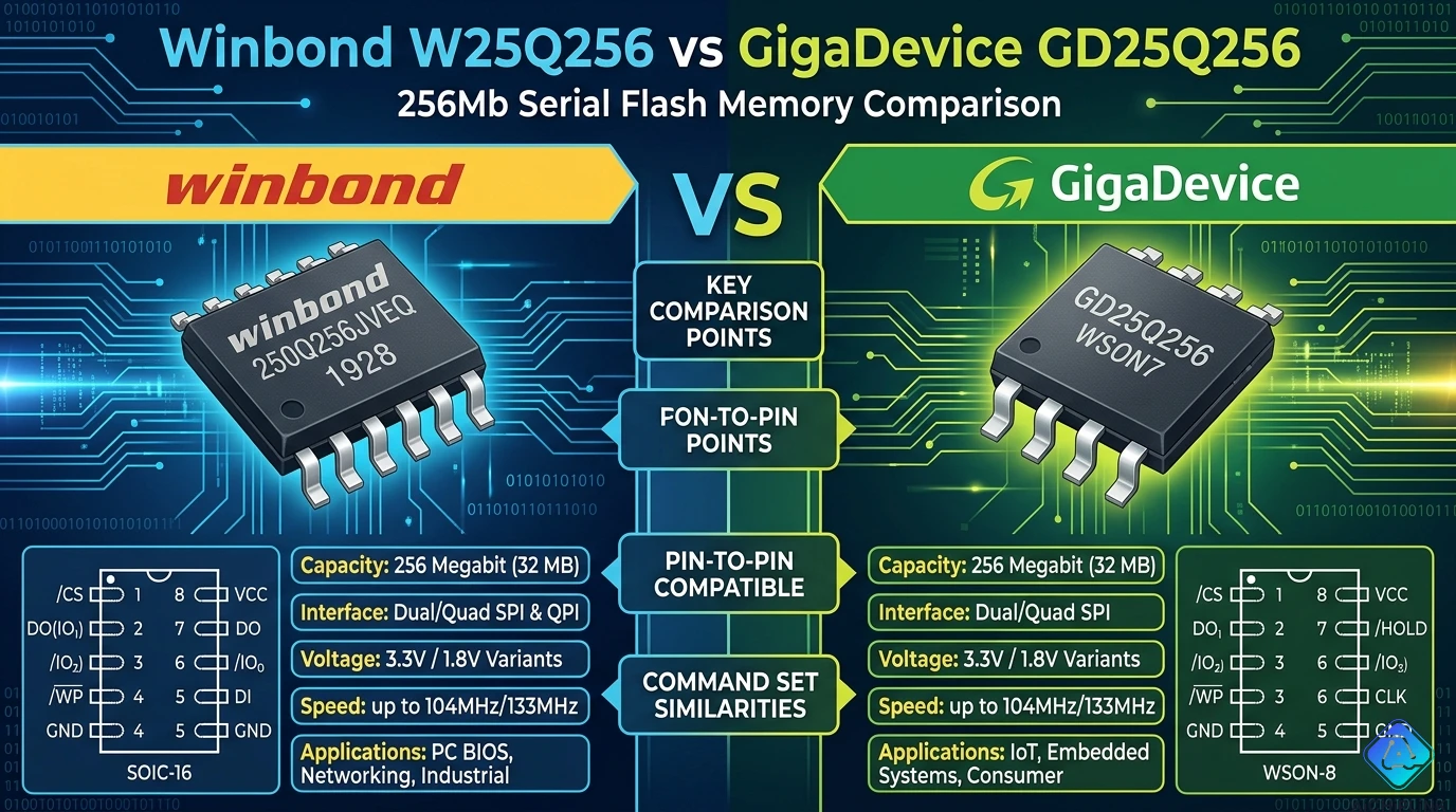
For this comparison: W25Q256JV (Winbond current production, 3.3V) vs GD25Q256E (GigaDevice current production, 3.3V). Both are JEDEC JESD216 SFDP-compliant.
3.0 Specifications Side by Side
| Parameter | W25Q256JV (Winbond) | GD25Q256E (GigaDevice) | Compatible? |
|---|---|---|---|
| Capacity | 256 Mbit (32 MB) | 256 Mbit (32 MB) | ✅ Identical |
| VCC range | 2.7V – 3.6V | 2.7V – 3.6V | ✅ Identical |
| Page size | 256 bytes | 256 bytes | ✅ Identical |
| Sector size | 4 KB | 4 KB | ✅ Identical |
| Block size | 64 KB | 64 KB | ✅ Identical |
| Total blocks | 512 | 512 | ✅ Identical |
| P/E endurance | 100,000 cycles | 100,000 cycles | ✅ Identical |
| Max SPI clock | 133 MHz | 133 MHz | ✅ Identical |
| Quad I/O throughput | 532 Mbps | 532 Mbps | ✅ Identical |
| JEDEC Manufacturer ID | 0xEF (Winbond) | 0xC8 (GigaDevice) | ❌ Different |
| Full RDID (9Fh) | EF 40 19 | C8 40 19 | ❌ Different |
| QE bit location | SR2 bit 1 | SR2 bit 1 | ✅ Identical |
| Default address mode | 3-byte (ADP=0) | 3-byte | ✅ Same default |
| 4-byte enter command | B7h (Enter 4-Byte Mode) | B7h (Enter 4-Byte Mode) | ✅ Same command |
| 4-byte exit command | E9h (Exit 4-Byte Mode) | E9h (Exit 4-Byte Mode) | ✅ Same command |
| Persistent 4-byte mode | Via ADP bit (S17) in SR3 | Via EN4B bit in register | ⚠️ Different register |
| 4-byte dedicated commands | Yes (12h, 13h, 21h, etc.) | Yes (dedicated set) | ✅ Broadly compatible |
| Block erase max (64KB) | 800 ms | 2,000 ms | ⚠️ GD slower |
| Security registers | 3 × 256 bytes | 3 × 1,024 bytes | ⚠️ Different size |
| SFDP support | Yes | Yes | ✅ Identical |
| Package (SOP-8) | 5.27×5.18mm | 5.27×5.18mm | ✅ Pin-compatible |
4.0 The 4-Byte Address Mode: Where the Real Differences Live
Both parts default to 3-byte address mode at power-up. Both require transitioning to 4-byte address mode to access addresses above 0xFFFFFF. Both use the same enter (B7h) and exit (E9h) commands. At this level they look identical. The differences are in the persistence and control of 4-byte mode across resets — and this is precisely where production failures occur.
W25Q256JV — the ADP bit (Status Register 3, S17):
Winbond provides a non-volatile ADP (Address Mode Pin/bit) in Status Register 3. When ADP = 0 (factory default), the chip powers up in 3-byte mode. When ADP = 1, the chip powers up in 4-byte mode. This setting persists across power cycles because it is stored in the non-volatile status register EEPROM.
The power-on address mode is visible to the host: the ADS (Address Mode Status) bit in the volatile Status Register 3 reflects the current address mode — the firmware can read it to confirm whether the chip is in 3-byte or 4-byte mode before issuing any address commands.
GD25Q256E — the EN4B approach:
GigaDevice uses a similar but not identical mechanism. The B7h Enter 4-Byte command works the same way and takes effect immediately. However, the register architecture for persistent 4-byte mode control differs from Winbond's SR3/S17 ADP bit. The Linux kernel's spi-nor driver patch that added GD25Q256 support explicitly handles GigaDevice's 4-byte address entry differently from Winbond's — the kernel needs manufacturer-specific code paths for each.
From a Linux kernel commit adding GD25Q256 support: the patch identifies GigaDevice flash by manufacturer ID 0xC8 and routes it through the Spansion/GigaDevice dedicated 4-byte command set branch — a separate code path from Winbond's implementation.
The practical consequence:
Firmware that:
- Issues B7h to enter 4-byte mode → works identically on both parts
- Reads back a status bit to confirm 4-byte mode is active → reads from different register locations on each manufacturer
- Relies on the flash remembering 4-byte mode across a power cycle via the non-volatile ADP bit → behavior differs between parts
- Powers up and assumes 3-byte mode (the safe default) and always re-issues B7h → works correctly on both parts
The safest approach — always issue B7h at firmware startup before accessing any address above 0xFFFFFF — is the only pattern guaranteed to work on both W25Q256 and GD25Q256 without manufacturer-specific code.
5.0 Firmware Compatibility: Same Chip, Different Behavior
Beyond 4-byte address mode, the firmware story at 256Mbit is similar to the 128Mbit comparison — with the additional 4-byte dimension.
What works identically:
- Standard SPI, Dual SPI, Quad SPI read commands (with 4-byte address prefix when in 4-byte mode)
- Page program (02h for 3-byte, 12h for 4-byte dedicated)
- Sector erase (20h for 3-byte, 21h for 4-byte dedicated)
- Block erase (D8h for 3-byte, DCh for 4-byte dedicated)
- QE enable: SR2 bit 1 on both (identical to each other, identical to the 128Mbit version)
- SFDP parameter discovery (both compliant)
- Deep power-down (B9h) and release (ABh)
What requires manufacturer detection:
- JEDEC ID: Winbond = EF 40 19 / GigaDevice = C8 40 19
- Persistent 4-byte mode register control
- Block erase timeout: GD max 2,000 ms vs Winbond max 800 ms
- Security register size: GD = 1,024 bytes each vs Winbond = 256 bytes each
The minimal safe firmware pattern for 256Mbit multi-vendor support:
// 1. Read JEDEC ID
uint8_t rdid[3];
spi_flash_read_jedec(rdid);
uint8_t mfr = rdid[0]; // 0xEF = Winbond, 0xC8 = GigaDevice

// 2. Verify capacity byte = 0x19 (256Mbit)
if (rdid[2] != 0x19) { /* handle unexpected density */ }

// 3. Enter 4-byte address mode unconditionally (works on both)
spi_flash_write_enable();
spi_flash_send_cmd(0xB7); // Enter 4-Byte Mode - same on both

// 4. All subsequent reads/writes/erases use 4-byte addresses
// Use dedicated 4-byte commands where available:
// Read: 13h (Fast Read 4-byte addr)
// Page Program: 12h
// Sector Erase 4KB: 21h
// Block Erase 64KB: DCh

// 5. Set erase timeout based on manufacturer
uint32_t block_erase_timeout_ms = (mfr == 0xC8) ? 3000 : 1500;
6.0 ⚠️ Four Ways This Swap Goes Wrong in Production
Pitfall 1: Firmware accesses only the bottom 16MB — silently
This is the most common failure mode and the hardest to detect. A 32MB flash is mounted. The firmware driver was written for a 16MB part, or the 32MB driver's 4-byte address mode was never validated because the developer only tested reads in the bottom 16MB. Everything works. The unit ships. Later, a firmware update writes to address 0x1000000 (byte 16,777,217 — the first byte of the upper 16MB). The write completes without error. The subsequent read returns 0xFF — the upper half was never programmed because the firmware was still sending 3-byte addresses and wrapping around. The failure is silent and only manifests in logs that correlate the write address with a read failure.
Fix: validate your flash driver against the full 32MB address range during bring-up. Write a test pattern to the last sector (address 0x1FF000) and verify the read-back before shipping.
Pitfall 2: Power cycle resets 4-byte mode, firmware does not re-issue B7h
A system powers up, firmware issues B7h, operates successfully. A watchdog reset or a power glitch resets the flash. The flash returns to 3-byte mode (the default). Firmware re-initializes but skips the B7h command (it was issued at first boot and the developer assumed it was persistent). All addresses above 0xFFFFFF now silently wrap or fail. The failure is intermittent, triggered by resets, and extremely difficult to reproduce deliberately.
Fix: Always re-issue B7h in the flash initialization sequence — every time, unconditionally. It takes one SPI transaction (2 bytes: WREN + B7h). There is no downside to issuing it redundantly.
Pitfall 3: JEDEC ID check fails, driver falls back to 16MB mode
A driver written for the W25Q256JV detects JEDEC ID EF 40 19, recognizes the 0x19 capacity byte as 256Mbit, and configures for 32MB operation. After a production substitution with GD25Q256, the driver reads C8 40 19, fails the manufacturer ID check against 0xEF, and falls back to a default 16MB (128Mbit) configuration. The upper 16MB is completely inaccessible. No error is reported — the firmware simply sees less flash than expected.
Fix: The JEDEC capacity byte 0x19 = 256Mbit regardless of manufacturer. If your driver uses the capacity byte (0x19) rather than manufacturer ID (0xEF/0xC8) to determine device size, this issue does not occur. Add GigaDevice 0xC8 to the manufacturer table alongside Winbond 0xEF.
Pitfall 4: Block erase timeout causes data corruption in background wear-leveling
The GD25Q256 maximum 64KB block erase time is 2,000 ms. Winbond maximum is 800 ms. A system with background wear-leveling running in a low-priority task sets its erase timeout at 1,200 ms. Under normal conditions GD erases complete in 200 ms (typical) and no timeout occurs. Under worst-case conditions — elevated temperature, end-of-life endurance, marginal supply voltage — a GD erase takes 1,800 ms and the driver's 1,200 ms timeout fires. The driver marks the sector as failed and retries, potentially issuing a new erase command while the first erase is still in progress — resulting in undefined behavior and potential data corruption. The failure is temperature-dependent, endurance-dependent, and statistically rare enough that it may pass all production testing before manifesting in the field.
Fix: Set block erase timeout to 3,000 ms minimum. This is generous enough to cover the GD25Q256 maximum (2,000 ms) with 50% margin.
7.0 Platform-Specific Notes: ESP-IDF, STM32 QSPI, Linux MTD
ESP32 / ESP-IDF:
Espressif explicitly lists both W25Q256 and GD25Q256 as supported chips in ESP-IDF. For 32MB flash on ESP32, ESP-IDF configuration requires enabling 32-bit address support for the full flash space. Important note from Espressif's documentation: space above 16MB can be used for data storage, but for code execution (mapping to the CPU's MMU/cache), additional experimental config flags are required and only certain ESP32 variants (specifically the S3) support mapping above 16MB. For most ESP32-based designs, if you need more than 16MB of accessible flash, the top 16MB is data-only — code must reside in the bottom 16MB.
Both W25Q256 and GD25Q256 are treated equivalently in ESP-IDF when SFDP detection is enabled. Without SFDP, check the ESP-IDF flash chip support list for your specific version.
STM32 QSPI / OSPI (HAL/QSPI driver):
STM32's QSPI and OSPI peripherals support 32-bit address mode when configured with AddressSize = QSPI_ADDRESS_32_BITS in the command structure. You must explicitly configure 4-byte address mode for all commands after issuing B7h to the flash. The STM32CubeIDE BSP flash drivers for W25Q256 use 4-byte addresses throughout — verify your driver is not using the 3-byte address template from a smaller W25Q variant.
For GD25Q256 on STM32, the same driver structure applies. Confirm the JEDEC ID detection in your HAL driver adds GigaDevice 0xC8 to the supported manufacturer table.
Linux MTD / spi-nor driver:
The Linux kernel spi-nor driver added GD25Q256 support via a specific patch that registers the chip under JEDEC ID 0xC84019 with SECT_4K | SPI_NOR_DUAL_READ | SPI_NOR_QUAD_READ flags. The patch also extends the 4-byte address routing to include GigaDevice manufacturer ID alongside Spansion — this is significant because without this patch, Linux will either fail to recognize GD25Q256 or configure it incorrectly for 4-byte addressing. If you are running a kernel older than the patch's merge date (2017), you will need to backport this entry to use GD25Q256 in a Linux MTD application. Check your kernel's drivers/mtd/spi-nor/spi-nor-ids.c for the gd25q256 entry to confirm support.
8.0 Decision Guide: When Each Is the Right Choice
Choose W25Q256JV when:
- Your firmware uses the non-volatile ADP bit mechanism to set persistent 4-byte mode at the register level
- Your driver relies on Winbond-specific status register bit locations for 4-byte mode status readback
- Your supply chain is Winbond-only and the BOM requires explicit manufacturer certification
- You need the faster worst-case block erase (800 ms vs 2,000 ms) for real-time applications
- You need security registers of exactly 256 bytes each (Winbond layout)
Choose GD25Q256E when:
- W25Q256 is on allocation and GigaDevice availability is better — provided your firmware is written to handle 4-byte addressing without manufacturer-specific assumptions
- Your driver uses SFDP for parameter discovery (both parts' SFDP is accurate and handles 4-byte addressing)
- Cost optimization is important — GD25Q256 typically prices 10–20% below W25Q256JV at production quantities
- Your platform is ESP32 (both officially listed in Espressif's supported chip list)
When NOT to substitute GD25Q256 for W25Q256 without firmware validation:
- Any design where firmware reads the ADP/ADS bit from a hardcoded Winbond-specific SR3 address to check 4-byte mode status
- Any system where the flash is expected to power up in 4-byte mode without firmware issuing B7h (only possible via the non-volatile ADP bit, whose control register differs)
- Any firmware with hardcoded JEDEC ID check expecting 0xEF
- Any system using Winbond security registers with exactly-256-byte addressing assumptions
9.0 Sourcing and Verification
Both W25Q256JV and GD25Q256E are available from authorized distributors including DigiKey, Mouser, Arrow, and LCSC. Typical pricing at 1,000-piece quantities: W25Q256JV ~$1.50–$2.20, GD25Q256E ~$1.20–$1.80.
Field verification at board level:
Issue the RDID command (9Fh) and check all three bytes:
| Expected | Meaning |
|---|---|
| EF 40 19 | Genuine W25Q256JV (Winbond, 256Mbit) |
| C8 40 19 | Genuine GD25Q256E (GigaDevice, 256Mbit) |
| Any XX XX 18 | 128Mbit device — wrong part or counterfeit |
| Any XX XX 17 | 64Mbit device — wrong part or counterfeit |
The capacity byte 0x19 = 256Mbit. If you read 0x18 (128Mbit), you have been shipped the wrong density — either a genuine 128Mbit part or a remarked 256Mbit counterfeit. Verify by writing to the last sector at address 0x1FF000 and confirming read-back returns your test pattern (not 0xFF or the data from the address-wrapped equivalent in the bottom 16MB).
For sourcing verified authentic W25Q256JV and GD25Q256E components with full traceability and competitive pricing, visit aichiplink.com.
10.0 Real Questions from Engineers Who Hit This
Q: I replaced W25Q256JV with GD25Q256 on our STM32 board. Now read/write works fine up to address 0xFFFFFF but everything above that returns 0xFF. Standard 3-byte reads return 0xFF instead of correct data above 16MB. Nothing crashes — it just reads zeros. What is wrong?
A: Your STM32 QSPI driver is not entering 4-byte address mode before accessing addresses above 0xFFFFFF. The fact that it works up to 16MB and fails above tells you exactly this — the driver sends 3-byte addresses, and the flash (whether Winbond or GigaDevice in 3-byte mode by default) wraps or ignores the access. The fix: add a B7h (Enter 4-Byte Mode) command to your flash initialization sequence, then confirm all read/write/erase commands send 4 address bytes. Also verify your STM32 QSPI configuration has AddressSize = QSPI_ADDRESS_32_BITS for all commands. This is not a W25Q256 vs GD25Q256 issue — the behavior is identical between them. It is a missing 4-byte mode initialization in your driver.
Q: Our firmware checks the ADP bit in Status Register 3 to confirm the flash is in 4-byte mode. This works on W25Q256JV but the same code reads garbage on GD25Q256. Why?
A: The ADP (Address Mode) bit is a Winbond-specific implementation in their Status Register 3 layout. GigaDevice's GD25Q256 uses a different register architecture for address mode control — the equivalent bit is not at the same position in SR3. When your firmware reads Winbond SR3 (via ReadSR3, command 15h) on the GD25Q256, it reads GigaDevice's SR3 which has a different bit map, and the ADP/ADS bit position does not correspond to Winbond's definition. The fix: do not read the ADP bit to verify 4-byte mode. Instead, verify 4-byte mode by writing a test pattern to an address above 0xFFFFFF and reading it back — if the read-back matches, 4-byte mode is active. This verification method works identically on both manufacturers.
Q: ESP-IDF says GD25Q256 is "supported" but I only see 16MB of flash accessible in my application. The remaining 16MB returns 0xFF on read. How do I enable the full 32MB?
A: There are two separate requirements for full 32MB access on ESP32. First, enable the 4-byte addressing configuration in menuconfig: under Component config → ESP-IDF Specific → SPI Flash driver, ensure the correct flash size is configured (32MB) and that 4-byte address mode is enabled. Second, understand ESP32's limitation: the upper 16MB of flash can be used for file system data or raw storage, but code execution (XIP) above the 16MB boundary requires enabling experimental config BOOTLOADER_CACHE_32BIT_ADDR_FLASH and is only supported on ESP32-S3. If your application uses the upper 16MB for a SPIFFS or LittleFS partition, verify your partition table has entries that fit within the device's 32MB. If you see 0xFF in the upper half, use the idf.py flash monitor to confirm the partition table covers the full 32MB and that the flash driver is initialized in 4-byte mode.
Q: Is there an Linux kernel device tree entry that works for both W25Q256 and GD25Q256 without specifying the manufacturer?
A: Yes — use the JEDEC-generic jedec,spi-nor compatible string with the capacity-based JEDEC ID. In your DTS:
flash@0 {
    compatible = "jedec,spi-nor";
    reg = <0>;
    spi-max-frequency = <50000000>;
    jedec-id = [ef 40 19]; /* W25Q256JV */
};
For GD25Q256, change jedec-id to [c8 40 19]. If you need to support both from a single device tree (for boards that may have either part populated), use the kernel's SFDP-based auto-detection path by listing jedec,spi-nor without a jedec-id property and allowing the kernel to probe via RDID at boot. Both W25Q256JV and GD25Q256E support SFDP (JEDEC JESD216), and the kernel's SFDP reader will correctly configure 4-byte addressing for both without manufacturer-specific logic.
11.0 Quick Reference Card
JEDEC IDs (RDID command 9Fh):
| Part | Full RDID | Capacity Byte |
|---|---|---|
| W25Q256JV (Winbond) | EF 40 19 | 0x19 = 256Mbit ✅ |
| GD25Q256E (GigaDevice) | C8 40 19 | 0x19 = 256Mbit ✅ |
| Any part returning XX 40 18 | Wrong density | 0x18 = 128Mbit ❌ |
4-Byte Address Mode — What Is the Same, What Is Different:
| Operation | W25Q256JV | GD25Q256E | Compatible? |
|---|---|---|---|
| Enter 4-byte mode | B7h | B7h | ✅ Yes |
| Exit 4-byte mode | E9h | E9h | ✅ Yes |
| Persistent 4-byte via non-vol bit | ADP bit in SR3 (S17) | Different register | ❌ Register location differs |
| Confirm mode via status bit | ADS bit in SR3 | Different register | ❌ Don't rely on this |
| Safest approach | Always issue B7h at init | Always issue B7h at init | ✅ Both |
The one rule that makes any 256Mbit driver work on both:
Always issue B7h (Enter 4-Byte Mode) in your flash init sequence — every boot, unconditionally.
Erase Timing:
| Operation | W25Q256JV Max | GD25Q256E Max | Set timeout to |
|---|---|---|---|
| Sector erase (4KB) | 400 ms | 400 ms | 600 ms |
| Block erase (64KB) | 800 ms | 2,000 ms | 3,000 ms |
| Chip erase | 400 s | 200 s | 450 s |
Swap Safety Checklist:
| Check | Result |
|---|---|
| Hardware footprint (SOP-8 / WSON) | ✅ Drop-in compatible |
| JEDEC ID lookup in firmware | ❌ Add 0xC8 (GigaDevice) |
| QE bit for Quad SPI | ✅ SR2 bit 1, same for both |
| B7h 4-byte mode enter | ✅ Both use B7h |
| ADP/ADS status bit readback | ❌ Different registers — don't use |
| Block erase timeout | ⚠️ Increase to 3,000 ms minimum |
| Security registers | ⚠️ GD = 1,024B each; WB = 256B each |
| SFDP auto-detection | ✅ Both compliant — use it |
| Full 32MB address test at bring-up | ✅ Always test address 0x1FF000 |
For sourcing W25Q256JV and GD25Q256E with verified authenticity and competitive pricing, visit aichiplink.com.

Written by Jack Elliott from AIChipLink.
AIChipLink, one of the fastest-growing global independent electronic components distributors in the world, offers millions of products from thousands of manufacturers, and many of our in-stock parts is available to ship same day.
We mainly source and distribute integrated circuit (IC) products of brands such as Broadcom, Microchip, Texas Instruments, Infineon, NXP, Analog Devices, Qualcomm, Intel, etc., which are widely used in communication & network, telecom, industrial control, new energy and automotive electronics.
Empowered by AI, Linked to the Future. Get started on AIChipLink.com and submit your RFQ online today!
Frequently Asked Questions
What is the main difference between W25Q256 and GD25Q256?
The key difference is how each chip handles 4-byte address mode persistence and status registers. Both support 32MB, but Winbond uses the ADP bit, while GigaDevice uses a different register structure—causing firmware compatibility issues.
Why does 32MB SPI flash require 4-byte addressing?
Because 24-bit addressing only supports up to 16MB, accessing the full 32MB requires 32-bit (4-byte) addressing. Without it, the upper 16MB becomes inaccessible or returns incorrect data.
Are W25Q256 and GD25Q256 pin-compatible replacements?
Yes, they are hardware pin-compatible, but not firmware-compatible by default. You must update JEDEC ID checks, 4-byte mode initialization, and timeout settings before swapping.
Why does my firmware fail above 16MB after replacing the flash chip?
This usually means 4-byte address mode is not enabled. The system continues using 3-byte addressing, causing reads/writes above 0xFFFFFF to fail or wrap incorrectly.


.png&w=256&q=75)


