Introduction
Every embedded system that runs on a battery eventually reaches the same design crossroads: how do you keep a microcontroller, RTC, or sensor interface alive in deep sleep for months or years, while still delivering a clean, well-regulated voltage when the system wakes up? The answer hinges almost entirely on one number — the LDO's quiescent current (IQ).
Standard LDOs consume 100–500 µA of IQ. In a standby system drawing 1 µA from its MCU, a 100 µA LDO wastes more power in its own biasing circuitry than the entire rest of the system. Over a one-year battery life target, that difference between a 100 µA LDO and a 1 µA ultra-low IQ device means the difference between a 500 mAh coin cell lasting two months versus two years.
The TPS7A2501DRVR from Texas Instruments is engineered precisely for this constraint. As a 300 mA, 18 V, ultra-low quiescent current, adjustable LDO voltage regulator with 1% output accuracy, power good output, internal soft start, and a compact 6-pin WSON (2 mm × 2 mm) package, it strikes the optimal balance between standby power, output capability, and integration for IoT nodes, smart meters, wearables, and any application where always-on supply efficiency defines the product's battery life.
According to TI's Power Management Design Center, ultra-low IQ LDOs have become one of the fastest-growing LDO sub-categories as energy efficiency regulations (EU ErP, US DOE standby power standards) tighten across consumer electronics, smart metering, and industrial IoT equipment. The TPS7A2501DRVR is TI's answer to this market need.
1.0 What Is the TPS7A2501DRVR? An Overview
The TPS7A2501DRVR is the adjustable-output, tape-and-reel variant of the TPS7A25 LDO family from Texas Instruments. It is the higher-current (300 mA) member of the TPS7A2x ultra-low IQ LDO series, designed for applications that need both meaningful load current capability and the lowest possible standby power.
Decoding the ordering code:
- TPS7A25 — Product family: ultra-low IQ, 18 V input, LDO linear regulator
- 01 — 300 mA current rating variant (the "01" suffix distinguishes this from the TPS7A2401 / TPS7A2402 lower-current variants)
- D — Adjustable output voltage (uses external R1/R2 feedback divider to set VOUT from 1.24 V to 17.64 V); contrast with fixed-voltage variants
- R — Tape-and-reel packaging
- VR — 6-pin WSON (2 mm × 2 mm) package with exposed thermal pad
The companion ordering code TPS7A2501DRVT is the same device in bulk tray packaging — otherwise electrically identical. The fixed-output variants (for standard voltages like 3.3 V, 5.0 V) omit the "D" in the package code and do not require R1/R2 resistors, offering simpler BOM and slightly lower IQ by eliminating the internal feedback amplifier's resistor bias.
"The TPS7A25 is an 18-V, low quiescent current, low-dropout (LDO) linear regulator. The low IQ performance makes the TPS7A25 an excellent choice for battery-powered or line-power applications that are expected to meet increasingly stringent standby-power standards." — Texas Instruments TPS7A25 Datasheet
2.0 Full Technical Specifications & LDO Architecture
2.1 Core Electrical Parameters
The following parameters are drawn from the TPS7A25 datasheet, at TJ = 25°C, VIN = VOUT + 0.5 V or 2.4 V (whichever is greater), IOUT = 1 mA, unless otherwise noted:
- Input Voltage Range (VIN): 2.4 V to 18 V
- Output Voltage Range (adjustable): 1.24 V to 17.64 V (set by external R1/R2)
- Output Current (IOUT): 300 mA maximum
- Dropout Voltage (VDO): 340 mV maximum at IOUT = 300 mA; typically < 200 mV at light load
- Internal Reference Voltage (VFB): 1.24 V ± 1% (over temperature and line)
- Output Voltage Accuracy: ±1% (over full temperature range, −40°C to +125°C)
- Quiescent Current (IQ): Ultra-low — see Section 2.2
- Feedback Bias Current (IFB): 10 nA typical
- Enable Pin (EN): Active-high, CMOS-compatible; internal pulldown resistor keeps device off when EN is floating
- Power Good Output (PG): Active-high, open-drain; goes high when VOUT is within ±10% of regulation target
- Soft Start: Internal — limits inrush current during startup
- Overcurrent Protection (OCP): Yes — current-limited pass transistor
- Overshoot Pulldown: Yes — actively discharges output on disable to prevent overshoot
- Thermal Shutdown (TSD): Yes — activates at approximately 165°C junction temperature
- Reverse Current Protection: Yes (limited; see Section 2.4)
- Operating Temperature Range: −40°C to +125°C
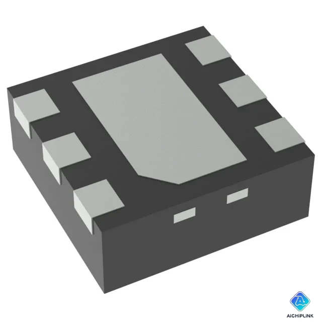
- Package: 6-pin WSON (DRV), 2 mm × 2 mm, 0.65 mm pitch, exposed thermal pad (EP)
- RoHS Compliant: Yes (Pb-free)
- ECCN: EAR99
- PSRR: > 40 dB at 1 kHz (typical, IOUT = 100 mA, COUT = 2.2 µF); see Section 5.2 for CFF enhancement
2.2 Ultra-Low Quiescent Current and Standby Power Analysis
The TPS7A2501DRVR's quiescent current specification is one of its most critical design parameters, and understanding how it compares to alternatives requires careful analysis.
The TPS7A25 family achieves quiescent currents in the low-µA range — significantly below the 50–100 µA of conventional LDOs, and competitive with the best ultra-low IQ devices on the market. The exact IQ figure varies with output voltage (lower VOUT generally gives lower IQ in the adjustable version due to the internal reference bias) and load current.
Battery life impact analysis:
Consider an IoT sensor node with the following power budget:
- MCU deep sleep: 2 µA
- Sensor interface standby: 5 µA
- LDO quiescent current: X µA
- Operating from a 1,000 mAh AA cell
| LDO IQ | Total standby current | Theoretical battery life |
|---|---|---|
| 100 µA (standard LDO) | 107 µA | ~1.07 years |
| 10 µA (low IQ LDO) | 17 µA | ~6.7 years |
| TPS7A2501DRVR (ultra-low IQ) | ~7–12 µA est. | ~9–17 years |
| TPS7A02 (25 nA IQ) | ~7.025 µA | ~16.2 years |
Note: TI does not publish a single IQ number for the TPS7A25 in its headline specifications; refer to the device's electrical characteristics table and IQ vs. VIN/IOUT performance curves in the datasheet for the exact figure at your operating conditions.
The key practical insight: in a system where the MCU itself draws only a few microamps in deep sleep, the LDO's IQ is often the dominant contributor to standby power consumption. Selecting the TPS7A2501DRVR over a standard 100 µA IQ LDO can extend battery life by a factor of 5–10× in light-load standby conditions.
2.3 Dropout Voltage, Input Range, and Efficiency
The 2.4 V to 18 V input range makes the TPS7A2501DRVR suitable for an exceptionally wide variety of power sources:
- Single-cell Li-Ion (3.0–4.2 V) → regulates down to 1.24 V output at any charge state
- 2-cell Li-Ion (6.0–8.4 V) → regulates to 3.3 V or 5 V outputs
- 12 V lead-acid or NiMH battery pack → directly regulated to logic supply rails
- USB 5 V input → regulated to 3.3 V, 2.5 V, or 1.8 V
- Industrial 12 V / 15 V bus → regulated to sensor supply rails
The 340 mV maximum dropout voltage at 300 mA enables high-efficiency linear regulation in near-dropout conditions. For example, regulating a 5 V output from a 5.4 V input:
Efficiency = VOUT / VIN = 5.0 / 5.4 = 92.6%
This is the fundamental efficiency advantage of a low-dropout regulator versus a standard LDO (which might require 1 V of headroom, giving only 83% efficiency in this scenario). Lower VDO also allows the LDO to remain in regulation as a battery discharges closer to its end-of-life voltage — extending the usable battery capacity.
Efficiency caveat: LDO efficiency equals VOUT / VIN only for the load current component; the IQ current always flows from VIN to GND at full VIN voltage. For very light loads where IQ approaches or exceeds the load current, LDO efficiency degrades significantly — this is why minimizing IQ is so important in standby-dominant applications.
2.4 Protection Features: Overcurrent, TSD, Soft Start, and Reverse Current
The TPS7A2501DRVR includes a comprehensive protection suite that enables robust operation without external protection components in most applications:
Overcurrent Protection (OCP): The internal pass transistor is current-limited — if the output current attempts to exceed the device's current limit threshold (typically 450–600 mA at 25°C, well above the 300 mA rated output), the device reduces the output voltage to limit current. This foldback-style behavior protects against short-circuit conditions without latching off.
Overshoot Pulldown: When the device is disabled (EN pulled low), an internal active pulldown circuit immediately discharges the output capacitor. This prevents voltage overshoot that could damage downstream ICs during power cycling, and ensures a clean, repeatable disable sequence in power-sequenced multi-rail systems.
Thermal Shutdown (TSD): Activates at approximately 165°C junction temperature, shutting off the pass transistor and reducing power dissipation. The TPS7A2501DRVR restores normal operation automatically once the die cools. TSD is a last-resort protection — see Section 5.1 for thermal management guidelines that prevent TSD from activating during normal operation.
Internal Soft Start: The output voltage ramps up smoothly during power-on, controlled by an internal timer rather than an external soft-start capacitor. This limits inrush current into the output capacitor during startup — particularly important when the input supply has limited current capability (coin cell, thin-film battery, or USB port with strict inrush current limits).
Reverse Current: The TPS7A2501DRVR has limited reverse current protection through the intrinsic body diode of the pass transistor. Conditions that create reverse current — such as powering the output from a secondary source while VIN is low, or strong output capacitor discharge into a collapsed input rail — can cause the body diode to conduct in reverse, potentially degrading the device over time. Review TI's application notes on reverse current for designs where this condition may occur.
3.0 Application Circuit Design
3.1 Output Voltage Setting: R1, R2, and CFF Selection
The TPS7A2501DRVR's output voltage is set by a resistor divider (R1 from VOUT to FB, R2 from FB to GND) according to:
VOUT = VFB × (1 + R1 / R2)
where VFB = 1.24 V is the internal reference voltage.
Design procedure:
Step 1: Choose R2. The feedback bias current IFB = 10 nA flows into the FB pin. For < 0.1% error contribution from IFB through R2, choose R2 ≤ VFB / (10 × IFB) = 1.24 / (10 × 10 nA) = 12.4 MΩ. In practice, TI recommends R1 + R2 ≤ 5 MΩ for the adjustable version. A good practical starting value is R2 = 1 MΩ — high enough to minimize quiescent current through the divider, low enough to overwhelm IFB error.
Step 2: Calculate R1 for the target VOUT: R1 = R2 × (VOUT / VFB − 1)
Step 3: Select nearest E96 standard resistor values and verify final VOUT.
Common VOUT settings (R2 = 1 MΩ):
| Target VOUT | R1 (calculated) | R1 (E96 nearest) | Actual VOUT | Error |
|---|---|---|---|---|
| 1.8 V | 451.6 kΩ | 453 kΩ | 1.804 V | +0.22% |
| 2.5 V | 1.016 MΩ | 1.02 MΩ | 2.506 V | +0.24% |
| 3.3 V | 1.661 MΩ | 1.65 MΩ | 3.287 V | −0.39% |
| 5.0 V | 3.032 MΩ | 3.01 MΩ | 4.977 V | −0.46% |
All values well within the ±1% over-temperature accuracy specification of the TPS7A2501DRVR — resistor tolerance adds to this, so use ≤ 1% tolerance resistors for R1 and R2.
CFF (Feedforward Capacitor): An optional capacitor CFF placed in parallel with R1 (from VOUT to FB) significantly improves PSRR, output noise, and transient response at the cost of slightly longer startup time. TI recommends CFF values between 10 nF and 100 nF for the adjustable version. Selecting CFF = 47 nF with R1 = 1.65 MΩ adds a zero to the feedback transfer function at:
f_zero = 1 / (2π × R1 × CFF) = 1 / (2π × 1.65M × 47n) ≈ 2.05 Hz
This extremely low-frequency zero effectively extends the LDO's loop bandwidth for noise rejection, improving PSRR by 10–20 dB at frequencies above 1 kHz — critical for applications where the LDO output powers analog sensors, ADC references, or RF circuits sensitive to power supply noise.
3.2 Power Good Output, Enable Pin, and Rail Sequencing
Power Good (PG) pin: The TPS7A2501DRVR's open-drain PG output asserts HIGH (through an external pull-up resistor, typically 100 kΩ to a logic supply) when VOUT is within approximately ±10% of the target regulation voltage. It goes LOW (PG pulls to GND through the internal FET) during:
- Device startup (before VOUT reaches the regulation threshold)
- Overcurrent / short-circuit conditions (when VOUT collapses)
- Thermal shutdown (when TSD activates)
- Device disabled (EN = LOW)
Practical PG uses:
- Connect PG to the RESET_n or POR (power-on reset) input of a microcontroller to hold the MCU in reset until the supply rail is fully established
- Use PG in a multi-rail power sequencing chain: LDO1's PG → EN of LDO2, enforcing a sequential startup order where LDO2 cannot start until LDO1's output is valid
- Connect PG to an MCU GPIO for firmware power-rail monitoring, enabling software-triggered reset on detected supply fault
Enable (EN) pin: The EN pin is active-high with a CMOS-compatible threshold and an internal pulldown resistor. This internal pulldown ensures the device remains off when EN is left floating — a critical safety feature that prevents the LDO from starting inadvertently when the control signal is not yet driven.
For always-on operation, tie EN directly to VIN (or to a logic supply that is present whenever the input supply is present). For software-controlled power gating, connect EN to an MCU GPIO — the TPS7A2501DRVR will power up when the GPIO goes high, and the internal soft start will ramp the output cleanly. The overshoot pulldown circuit will discharge the output rapidly when EN is pulled low, preventing voltage spikes on the load.
3.3 Battery-Powered IoT, Wearable, and Smart Meter Applications
The TPS7A2501DRVR's combination of ultra-low IQ, 18 V input range, and 300 mA output current targets several high-growth IoT battery-powered application categories:
IoT sensor nodes (LoRaWAN, NB-IoT, Zigbee): A typical LoRa sensor node spends > 99.9% of its time in deep sleep, waking every few minutes to transmit a sensor reading. The TPS7A2501DRVR powers the MCU and radio from a primary lithium battery (3.6 V AA, 3.0–3.6 V operating range), with its ultra-low IQ dominating the sleep-state current budget. During the brief transmission burst (~300 mA peak for LoRa transmit), the 300 mA output current satisfies the peak demand without dropout.
Smart utility meters (gas, water, electricity): Smart meters operate from non-rechargeable lithium primary cells designed to last 10–15 years. With meter reading intervals of 15 minutes to 1 hour, the meter's electronics are in standby for > 99.9% of their lifetime. The TPS7A2501DRVR's ultra-low IQ reduces the standby power contribution of the LDO to a negligible fraction of the cell's self-discharge rate, enabling the full 10–15 year cell life.
Wearable electronics (fitness trackers, medical patches, hearing aids): Wearables typically operate from small LiPo cells (100–500 mAh), requiring every microwatt of standby power to be justified. The TPS7A2501DRVR's 2 mm × 2 mm WSON footprint fits into the ultra-compact PCBs of wearable devices while delivering sufficient current for BLE radio transmissions and sensor readouts.
Industrial wireless sensors: Remote industrial sensors (pressure, temperature, vibration) in areas without grid power must operate from batteries or energy harvesters for years. The TPS7A2501DRVR's 2.4 V to 18 V input range accommodates everything from supercapacitor energy harvesters (2.5–5 V) to multi-cell lithium packs (7.2–18 V) in a single LDO solution.
3.4 Always-On MCU Supply and Standby Rail Design
In many embedded systems, one power rail must remain active at all times — powering the MCU's RTC, backup SRAM, BLE stack, or security co-processor — while other rails (CPU core, RF radio, peripherals) are switched off during sleep to save power. The TPS7A2501DRVR is ideally suited as this always-on rail regulator:
- Ultra-low IQ ensures the always-on rail itself consumes minimal power
- 300 mA provides enough current for the MCU to operate normally when it wakes from sleep without requiring a separate higher-current regulator for wake-up current spikes
- Power Good monitors the always-on rail and drives the MCU's reset input — ensuring the MCU only starts execution when its supply is fully stable
- 18 V input allows the always-on rail to be powered directly from the battery bus without an intermediate converter, simplifying the power architecture
- Internal soft start prevents inrush current spikes on initial power-up that could reset or damage sensitive MCU peripherals
For an always-on 3.3 V rail from a 2-cell Li-Ion pack (6.0 V minimum fully discharged):
- R2 = 1 MΩ, R1 = 1.65 MΩ → VOUT ≈ 3.287 V (within ±1% of 3.3 V)
- Minimum VIN for regulation: VOUT + VDO = 3.3 + 0.34 = 3.64 V — well within the 6.0 V minimum battery voltage
- Maximum VIN: 18 V > 8.4 V fully charged — no overvoltage concern
4.0 TPS7A2501DRVR vs. Competing Ultra-Low IQ LDOs
4.1 TPS7A2501DRVR vs. TPS7A24, TPS7A02, LP5907, and XC6222
| Feature | TPS7A2501DRVR | TPS7A24DRVR | TPS7A02DRVR | LP5907MFX-3.3 | XC6222 (Torex) |
|---|---|---|---|---|---|
| Max Output Current | 300 mA | 200 mA | 200 mA | 300 mA | 300 mA |
| Input Voltage Range | 2.4–18 V | 2.4–18 V | 1.7–5.5 V | 2.2–5.5 V | 1.7–5.5 V |
| Output Voltage | Adj. 1.24–17.64 V | Adj. 1.24–17.75 V | Adj. 0.8–5.0 V | Fixed 3.3 V | Fixed/Adj. 0.9–5.0 V |
| Quiescent Current | Ultra-low µA | Ultra-low µA | 25 nA (!) | 75 µA | ~40 µA |
| Accuracy | ±1% | ±1.25% | ±2% | ±2% | ±1% |
| Dropout @ rated IOUT | 340 mV / 300 mA | 250 mV / 200 mA | ~600 mV / 200 mA | 280 mV / 300 mA | ~200 mV / 300 mA |
| Power Good | Yes | No | Yes | No | No |
| Enable Pin | Yes | Yes | Yes | Yes | Yes |
| Soft Start | Internal | Internal | Internal | None | None |
| Overshoot Pulldown | Yes | Yes | Yes | No | No |
| Reverse Current Protect | Partial | Partial | Full | None | None |
| Package | WSON 6 (2×2mm) | WSON 6 (2×2mm) | WSON 6 (2×2mm) | SOT-23-5 | SOT-25 |
| AEC-Q100 | No | No | No | No | No |
| Price/Unit (1k) | ~$0.40–$0.55 | ~$0.40–$0.55 | ~$0.55–$0.70 | ~$0.35–$0.50 | ~$0.20–$0.35 |
Key selection guidance:
- Need 300 mA, 18 V input, adjustable output, power good, ultra-low IQ → TPS7A2501DRVR — this device; the widest VIN range in its class, with PG output for sequencing and the best combination of IQ, accuracy, and current capability for IoT and industrial applications
- Need 200 mA, 18 V input, same family, lower cost → TPS7A24DRVR — sister product, 200 mA, 250 mV dropout, same WSON package; choose when 200 mA is sufficient and power good is not needed
- Need absolute minimum IQ (25 nA!) for ultra-long battery life → TPS7A02DRVR — TI's nanopower LDO; the lowest-IQ product in TI's portfolio, but limited to 5.5 V input (suitable only for single-cell Li-Ion or low-voltage applications), and ±2% accuracy vs. ±1% for TPS7A2501DRVR
- Need fixed 3.3 V output, no resistors required, lower cost → LP5907MFX-3.3 — TI's fixed-output low-noise LDO; 75 µA IQ (much higher than TPS7A2501DRVR in standby), no power good, but excellent PSRR and noise for noise-sensitive analog loads
- Need lowest cost, VIN < 5.5 V only → XC6222 — Torex ultra-compact LDO, competitive pricing, adequate for simple 3.3 V / 5 V applications from Li-Ion, but no PG, no overshoot pulldown, and higher IQ than TPS7A2501DRVR
4.2 Ordering Codes, Package Options & Availability
The TPS7A25 family ordering system can be initially confusing — here is a complete decoder:
TPS7A2501 = 300 mA, adjustable output (D = adjustable, no D = fixed) TPS7A2401 = 200 mA, adjustable output
Package suffix:
- DRVR = 6-WSON, 2 mm × 2 mm, exposed pad, tape-and-reel (the subject of this article)
- DRVT = 6-WSON, 2 mm × 2 mm, exposed pad, bulk tray (same device, tray packaging)
Fixed-output variants (no external resistors needed): TPS7A2501x033 (3.3 V), TPS7A2501x050 (5.0 V), etc. — the voltage is encoded in the ordering suffix.
Availability:
- Authorized distributors: DigiKey, Mouser, Arrow, Avnet, LCSC
- Typical unit pricing: ~$0.40–$0.55 USD (1k+ quantity, tape-and-reel)
- Lead time: Generally in-stock at major distributors; 8–14 week lead times possible during supply-constrained periods
- RoHS: Fully compliant (Pb-free)
- ECCN: EAR99
- Evaluation module: TPS7A25EVM (Texas Instruments evaluation board for TPS7A25 family, ~$49 USD)
For competitive pricing, verified authentic TI inventory, and volume procurement support, visit aichiplink.com — TPS7A2501DRVR listing.
5.0 PCB Layout and Design Optimization
5.1 6-WSON Layout, Exposed Pad, and Thermal Management
The 6-pin WSON (DRV) package measures 2 mm × 2 mm with a 0.65 mm lead pitch and a central exposed pad (EP). In a package this small, layout discipline is critical:
Exposed pad (EP) soldering: The EP provides both the primary ground connection and thermal path. It must be soldered to the PCB ground plane — a cold or open EP solder joint increases the effective junction-to-ambient thermal resistance by a factor of 3–5×, severely limiting maximum power dissipation.
Place 4 thermal vias (0.2 mm drill, 0.4 mm pad) in a 2×2 grid under the EP, connecting the top-layer ground copper to the inner or bottom ground plane. This is the single most important thermal management step for the TPS7A2501DRVR.
Power dissipation and thermal limits:
P_D = (VIN − VOUT) × IOUT + VIN × IQ
For VIN = 12 V, VOUT = 3.3 V, IOUT = 300 mA:
P_D = (12 − 3.3) × 0.3 = 8.7 V × 0.3 A = 2.61 W
With θJA ≈ 74°C/W (6-WSON on standard 2-layer PCB), junction temperature rise: ΔTJ = P_D × θJA = 2.61 × 74 = 193°C → exceeds TSD threshold!
This calculation reveals a critical design constraint: at high input-to-output voltage differences, the TPS7A2501DRVR cannot deliver rated 300 mA continuously. The maximum safe load current at a given VIN and TA is:
IOUT_max = (TJ_max − TA) / (θJA × (VIN − VOUT))
At VIN = 12 V, VOUT = 3.3 V, TA = 25°C, TJ_max = 125°C:
IOUT_max = (125 − 25) / (74 × 8.7) = 100 / 644 ≈ 155 mA
The full 300 mA is only available when (VIN − VOUT) is small (near-dropout operation). For high VIN–VOUT designs requiring full 300 mA, a pre-regulation DCDC converter feeding the LDO at VOUT + 0.5 V is the recommended architecture.
5.2 CFF Feedforward Capacitor: PSRR, Noise, and Transient Trade-Offs
The feedforward capacitor CFF, placed in parallel with R1 (from VOUT to FB pin), is one of the most powerful and underutilized design tools available for LDO optimization. TI's application note "Pros and Cons of Using a Feedforward Capacitor with a Low-Dropout Regulator" (SLVA289) provides the complete analysis; the key trade-offs are:
Benefits of CFF:
- Improved PSRR: CFF adds a feedback zero that extends the LDO's loop bandwidth, allowing the error amplifier to reject input noise at higher frequencies. At 10 kHz with CFF = 47 nF, PSRR can improve by 10–20 dB versus no CFF — critical for rejecting switching noise from an upstream DCDC converter
- Lower output noise: The extended bandwidth reduces the noise contribution of the internal reference by increasing the frequency at which the loop begins to attenuate noise
- Better load transient response: Faster loop response reduces the amplitude and duration of output voltage deviations during load current steps
Trade-offs of CFF:
- Slower startup: CFF must charge through R1 during startup, extending the soft-start ramp time. With R1 = 1.65 MΩ and CFF = 100 nF: τ = R1 × CFF = 1.65M × 100n = 165 ms — a 165 ms soft-start time that may be unacceptable if fast startup is required
- Increased startup inrush: The CFF charging current flows from VOUT into the FB pin during startup — with large CFF and high VOUT, this inrush can be significant
Recommended CFF range: 10 nF to 100 nF. For battery-powered applications where startup time is not critical, 47 nF is a good general-purpose choice. For applications requiring fast startup (< 10 ms), limit CFF to ≤ 10 nF or omit it entirely.
5.3 Input and Output Capacitor Selection
The TPS7A2501DRVR is stable with small ceramic capacitors — a key advantage for compact PCB designs:
Input capacitor (CIN):
- Minimum recommended: 1 µF ceramic (X5R or X7R, ≥ 25 V rating at VOUT + 20% margin)
- Typical value: 2.2 µF (provides adequate bulk for fast load transients and filters source impedance)
- Placement: As close as possible to the VIN pin, with the return path directly to GND via a short low-inductance trace or via
Output capacitor (COUT):
- Minimum for stability: 1 µF ceramic (X5R or X7R)
- Maximum recommended: 50 µF effective capacitance — higher values increase startup time and may cause stability issues in some operating conditions
- Typical value: 2.2 µF — balances transient response, stability, and board area
- Derating note: X7R ceramic capacitors derate significantly with DC bias voltage. A 10 µF 10 V X7R capacitor at VOUT = 5 V may have an effective capacitance of only 5–6 µF. Always verify effective capacitance at the actual operating voltage using the capacitor manufacturer's derating curves.
Capacitor ESR: The TPS7A2501DRVR is designed for use with low-ESR ceramic capacitors — unlike older LDOs that required an output capacitor ESR in a specific range (0.1–10 Ω) for stability. Aluminum electrolytics with high ESR are not appropriate and may cause oscillation.
6.0 How to Source Authentic TPS7A2501DRVR Units
The TPS7A2501DRVR's small package size (2 mm × 2 mm WSON) and relatively modest unit price make it susceptible to counterfeiting — a counterfeit device may regulate voltage approximately but with incorrect IQ (consuming 1 mA instead of a few µA), missing power good functionality, incorrect thermal shutdown temperature, or degraded accuracy outside the ±1% specification. In a battery-powered IoT device, a counterfeit LDO with 10× higher IQ could reduce the product's battery life from three years to three months — a defect that may not be discovered until products are in the field.
Sourcing guidelines:
- Purchase from TI authorized distributors only: DigiKey, Mouser, Arrow, Avnet, and Newark are Texas Instruments' authorized stocking distributors. These channels guarantee genuine TI parts with full manufacturing lot traceability.
- Verify package marking: The TPS7A2501DRVR's 2 mm × 2 mm WSON package carries a date/lot code and device marking. At this package size, markings are extremely small — verify under 10× magnification that characters are crisp and laser-etched, not ink-printed or transferred labels.
- Reel label inspection: Authentic TI tape-and-reel reels carry TI's reel label with the full part number (TPS7A2501DRVR), date code, quantity, and country of origin. Cross-reference the label barcode with the TI part number format.
- Functional verification: In a simple test circuit with R1 = 1.65 MΩ, R2 = 1 MΩ, CIN = COUT = 2.2 µF, VIN = 5 V: measure VOUT (should be 3.287 ± 1% = 3.255–3.320 V), measure IQ with IOUT = 0 µA (disconnect load and measure IIN − estimated current through R1/R2 divider). Measure PG logic level — should be HIGH through pull-up resistor at stable output. A device reading IQ > 100 µA at no load, or VOUT outside ±2%, should be rejected.
- Request CoC for production quantities: For volume procurement, require a Certificate of Conformance with TI lot date code traceability before acceptance.
For verified authentic Texas Instruments TPS7A2501DRVR inventory with competitive pricing and expert technical support, visit aichiplink.com.
7.0 Conclusion
The TPS7A2501DRVR delivers an exceptional combination of capabilities that define the modern ultra-low IQ LDO for battery-powered and always-on IoT applications: a 2.4 V to 18 V input range that accommodates nearly every primary and secondary battery chemistry on the market; 300 mA output current that handles the peak current demands of radio transmissions and sensor activations; ±1% output accuracy over temperature that meets precision MCU reference requirements; power good output that enables clean rail sequencing and supervised startup; and an ultra-low quiescent current that can reduce the LDO's standby power contribution to a fraction of the system's total standby budget.
The adjustable output variant (TPS7A2501DRVR) provides complete voltage flexibility from 1.24 V to 17.64 V via two external resistors, with the optional CFF feedforward capacitor offering a practical lever for trading startup speed against improved PSRR and transient performance. The thermal analysis in this guide makes clear that the LDO's practical current capability at high input-to-output voltage differences requires careful design — but in its intended operating regime (near-dropout, battery-powered, light-to-moderate load), the TPS7A2501DRVR is one of TI's most capable and efficient solutions for keeping embedded systems powered cleanly at the lowest possible standby energy cost.
Ready to evaluate the TPS7A2501DRVR? Source verified authentic Texas Instruments inventory, explore competitive volume pricing, and access TPS7A25EVM evaluation module support at aichiplink.com — TPS7A2501DRVR.

Written by Jack Elliott from AIChipLink.
AIChipLink, one of the fastest-growing global independent electronic components distributors in the world, offers millions of products from thousands of manufacturers, and many of our in-stock parts is available to ship same day.
We mainly source and distribute integrated circuit (IC) products of brands such as Broadcom, Microchip, Texas Instruments, Infineon, NXP, Analog Devices, Qualcomm, Intel, etc., which are widely used in communication & network, telecom, industrial control, new energy and automotive electronics.
Empowered by AI, Linked to the Future. Get started on AIChipLink.com and submit your RFQ online today!
Frequently Asked Questions
What is the difference between TPS7A2501DRVR and fixed-output versions?
The TPS7A2501DRVR is an adjustable LDO from Texas Instruments that requires two external resistors to set the output voltage between about 1.24 V and 17.6 V. Fixed-output variants integrate the feedback resistors internally for preset voltages like 3.3 V or 5 V, simplifying the design and reducing the component count.
How does the TPS7A2501DRVR power-good pin work?
The power-good (PG) pin is an open-drain output that indicates whether the regulator output is in regulation. When the output voltage is stable, the pin goes high through an external pull-up resistor; when the voltage is out of range or during startup, the pin is pulled low.
Can TPS7A2501DRVR run from a 3.6 V lithium battery?
Yes. The TPS7A2501DRVR supports an input voltage range of 2.4 V to 18 V, so it can operate from common 3.6 V lithium primary cells. Designers should still verify the dropout voltage to ensure regulation is maintained as the battery voltage approaches end-of-life.
Is TPS7A2501DRVR suitable for RF circuits?
The regulator provides moderate PSRR, which is typically sufficient for battery-powered RF modules such as BLE or LoRa devices. However, when used after a switching regulator, additional filtering or a higher-PSRR LDO may be required for very noise-sensitive RF circuits.
What temperature can TPS7A2501DRVR operate at full current?
The maximum ambient temperature at 300 mA output current depends on input-to-output voltage drop and PCB thermal design. With small voltage differences (for example 3.7 V to 3.3 V), the device can operate safely at very high ambient temperatures within the 125°C junction limit, assuming proper PCB heat dissipation.