What Is ADBMS1818ASWZ? Why isoSPI Is Not SPI, and Why That Matters in a 400V Battery Pack
The ADBMS1818ASWZ communicates over something called isoSPI. If you are familiar with SPI — the ubiquitous four-wire serial interface found on microcontrollers everywhere — you might reasonably assume isoSPI is SPI with some kind of isolation transformer added to one of the lines. That assumption gets the function right but misses the mechanism entirely, and missing the mechanism leads to real design errors in high-voltage battery management systems.
Standard SPI requires both devices to share a common ground reference. In a battery stack where 18 cells are connected in series, the "ground" of each monitoring IC is the negative terminal of its local cell group — not the system ground. The bottom IC in a 400V stack sits 400V above the top IC's local reference. There is no common ground between them. Running SPI signals between ICs that are floating at different potentials relative to each other — and to the host microcontroller — would require either multiple isolated power supplies and isolated gate drivers for each interface, or some other isolation scheme that adds enormous BOM cost.
isoSPI is Analog Devices' answer to this problem. Instead of multi-wire parallel data signals that require a common ground reference, isoSPI encodes the data as a differential current pulse on a single twisted pair of wires. The differential encoding means the signal is defined by the difference between two conductors, not between one conductor and ground — so ground potential does not matter. An isolation transformer at each end of the link completes the galvanic isolation. The twisted pair can run up to 100 meters, is inherently immune to common-mode noise (which is enormous in a high-voltage switching environment), and requires only two wires between monitoring ICs regardless of how many are in the chain.
Understanding isoSPI is understanding why ADBMS1818ASWZ is designed the way it is, and why every battery stack monitor that needs to communicate across floating voltage domains eventually arrives at a similar solution.
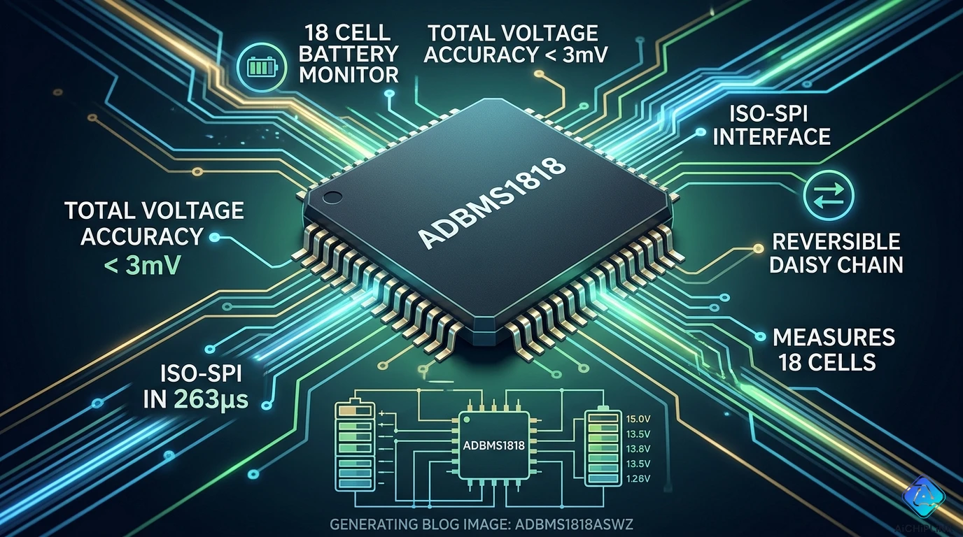
1.0 Part Number Decoded: ADBMS1818ASWZ
ADBMS — Analog Devices Battery Management Series prefix. Analog Devices uses this prefix for their advanced multicell battery stack monitor family, which includes the ADBMS1818 and related devices. The "AD" is Analog Devices' general product prefix; "BMS" identifies the battery management function.
1818 — Product identifier. The 18-18 structure reflects the device's primary specification: 18 cell inputs, with the architecture designed around an 18-channel ADC front end. (It is not, as sometimes assumed, a reference to two 18-cell measurements running simultaneously — the device has one ADC core that sequences through 18 channels.)
A — Silicon revision: A = improved version of the base ADBMS1818. The ADBMS1818A (with the "A" suffix before the package code) incorporates specific analog and digital improvements over the original ADBMS1818 silicon — primarily refined ADC linearity and improved noise performance at the measurement front end. The "A" here is a silicon revision indicator embedded in the base product name, not part of the ordering suffix.
SWZ — Ordering suffix encoding package, variant, and compliance:
- S = Standard production version (as opposed to engineering samples or special screening)
- W = Package code indicating the specific eLQFP (enhanced LQFP with exposed pad) variant
- Z = RoHS compliant, lead-free (Pb-free) finish — consistent with Analog Devices' convention where Z suffix indicates lead-free/RoHS compliance
Package: 64-lead eLQFP (enhanced Thin Quad Flat Pack with exposed thermal pad), 10 mm × 10 mm body, 0.5 mm lead pitch
Ordering variants on the same die:
| Part number | Quantity per reel | Notes |
|---|---|---|
| ADBMS1818ASWZ | Tube (tray) | Standard production, this article's subject |
| ADBMS1818ASWZ-R7 | 750/reel | Tape-and-reel, smaller reel |
| ADBMS1818ASWZ-RL | 2,500/reel | Tape-and-reel, standard production reel |
| ADBMS1818ASWAZ | Tray | Alternate tray packaging designation |
All variants are electrically identical — the suffix encodes only packaging and reel quantity.
2.0 Specifications: What the ADBMS1818 Measures and How Accurately
Cell voltage measurement:
- Number of inputs: 18 (C0–C18 differential cell voltage inputs)
- Cell voltage range: 0 V to 5 V per cell (covers Li-ion ~2.5–4.2V, LFP ~2.5–3.65V, NMC, lead-acid, and most other chemistries)
- Total Measurement Error (TME): < 3.0 mV maximum across all cells, all temperatures
- ADC resolution: 16-bit Δ-Σ (delta-sigma) with programmable third-order sinc filter
- LSB size: Approximately 100 µV (the 16-bit ADC over the 0–5V range)
- Measurement time (all 18 cells): 290 µs in the fastest mode (7 kHz filter)
- Noise reduction modes: Multiple filter bandwidths selectable (27 Hz to 7 kHz) — lower bandwidth = more filtering = better noise rejection but longer measurement time
Why 3 mV TME matters for SoC accuracy:
State of Charge estimation in lithium cells uses the cell voltage as one input to the SoC algorithm. A 3 mV error on a cell with a full-charge voltage of 4.2V and a 3.0V cutoff represents an error of 3 mV / 1200 mV = 0.25% of the usable voltage range. For a 100 kWh battery pack, this translates to approximately 250 Wh of uncertainty in the SoC estimate — relevant for range prediction in EVs. Each millivolt of measurement error directly affects SoC accuracy; the ADBMS1818's sub-3 mV specification is one of its primary competitive differentiators.
Auxiliary measurements:
- GPIO inputs (9 total): Configurable as analog inputs (0–3V range) for NTC thermistors, Hall-effect sensors, or other analog sensors; or as digital I/O; or as I²C/SPI master outputs for external sensor ICs
- Internal temperature sensor: On-chip die temperature measurement
- Supply voltage measurement: Monitors VREG (internal 5V regulator output) and VDD (stack supply input)
Cell balancing:
- Passive balancing: Each cell input (C1–C18) has an associated balancing MOSFET gate output (S1–S18)
- Maximum balancing current: Up to 200 mA with external resistor selection
- PWM control: Per-cell duty cycle programmable for heat-managed balancing
- Discharge timer: On-chip timer allows timed balancing sequences without continuous host intervention
Communication:
- isoSPI: 1 Mb/s isolated serial, single twisted pair, up to 100 meters
- Bidirectional daisy chain: Both "upstream" and "downstream" communication paths maintained simultaneously — if one direction fails (broken wire), the other direction still functions
- SPI (direct): Standard SPI also available for direct host connection (not isolated)
Power:
- Stack supply (VCC–V−): 16V to 90V (the total voltage of the cells being monitored, from the bottom cell's negative terminal to the top cell's positive)
- Internal 5V regulator: On-chip LDO generates 5V from VCC for the device's own logic and for driving external circuitry from the GPIO pins
- Active mode current: Approximately 4–5 mA from the stack supply
- Sleep mode current: 6 µA — enables long-term standby monitoring with minimal battery drain
Interface and protection:
- ESD protection: All cell inputs have built-in input protection
- Temperature range: −40°C to +85°C
3.0 The Core Concept: How isoSPI Works and Why It Solves the Floating Ground Problem
The problem isoSPI solves:
In a series battery stack of N groups of 18 cells, each ADBMS1818 is referenced to the negative terminal of its cell group. If the bottom group's negative terminal is at 0V (system ground), and each group spans approximately 18 × 3.6V = 64.8V (for Li-ion), then:
- IC1 (bottom group): referenced to 0V
- IC2 (second group): referenced to 64.8V above system ground
- IC3 (third group): referenced to 129.6V above system ground
- IC4 (fourth group): referenced to 194.4V above system ground
Any signal path that creates a direct electrical connection between these ICs must bridge these voltage differences. Standard SPI (with shared MISO/MOSI/CLK/CS wires between a common-referenced bus) cannot do this — it would place 64.8V, 129.6V, or higher potential directly across the SPI signal lines between adjacent ICs.
How isoSPI encodes data without a common ground:
isoSPI replaces the parallel voltage-referenced data signals of standard SPI with a differential current pulse on a single twisted pair. The protocol works as follows:
A logic "1" is encoded as a short (approximately 1 µs) positive current pulse on the twisted pair. A logic "0" is encoded as a negative current pulse (current flows in the opposite direction). A third state (no current pulse) represents an idle/gap period between bits.
At each end of the isoSPI link, a pulse transformer (isolation transformer) couples the differential current pulse magnetically from one side to the other. The transformer has no DC path — it provides galvanic isolation between the two sides. The secondary side of the transformer detects the differential pulse and reconstructs the original SPI data.
The key insight: Because the data is encoded as a differential current pulse (difference between the two conductors), and because a transformer is used for coupling, the absolute voltage of either conductor relative to ground is irrelevant. A 65V common-mode voltage on the twisted pair — because IC2 sits at 65V above system ground — simply appears as an offset on both conductors simultaneously and is rejected. Only the differential component (the actual data pulse) is transferred.
Why twisted pair matters:
The 100-meter cable length specification assumes a twisted pair (not individual wires or a PCB trace). Twisting the two conductors ensures that any externally induced noise affects both conductors equally (common-mode noise), which the differential receiver rejects. In an EV or energy storage environment where inverters, motor drives, and high-current switching create intense electromagnetic noise, the twisted pair's common-mode rejection is what makes 100-meter cable runs practical.
4.0 Real Circuit Application: A 400V Battery Stack with Daisy-Chained ADBMS1818s
A 400V automotive traction battery using prismatic lithium-ion cells (nominal 3.6V per cell) requires approximately 111 cells in series (400V / 3.6V = 111 cells). Grouped into six 18-cell monitoring zones (6 × 18 = 108 cells, covering up to 108 × 4.2V = 454V full-charge), six ADBMS1818 devices are needed.
System architecture:
The six ADBMS1818 devices are connected in a daisy chain: the host microcontroller (e.g., an automotive-grade STM32 or Renesas RH850) connects via standard SPI to the first device in the chain. The first device's isoSPI port connects via twisted pair to the second device's isoSPI port. The second to the third, and so on through the sixth device.
The host sends a single broadcast command on its SPI interface. The first ADBMS1818 receives the command, executes its local measurement, and relays the command upstream through its isoSPI port to the next device. Within 290 µs, all 108 cells in the stack have been measured simultaneously. The results are read back through the chain in sequence.
The bidirectional reliability advantage:
The daisy chain operates bidirectionally — data can flow from host → device1 → device2 → ... → device6, and also from device6 → device5 → ... → device1 → host. If the twisted pair cable between device3 and device4 is cut (a real concern in automotive crash scenarios or assembly damage), the chain can reconfigure: the host continues communicating with device1, device2, device3 from the bottom, and simultaneously communicates with device6, device5, device4 from the top through the daisy chain's reverse direction. All devices remain accessible even with one broken link.
Temperature monitoring:
Each ADBMS1818 has 9 GPIO pins. In a typical BMS design, 3–5 GPIO pins per IC are used as analog inputs connected to NTC thermistors (10 kΩ at 25°C) distributed across the cell group — mounted between cells, on busbars, or on the module housing. The ADBMS1818 measures the thermistor voltage using its internal ADC (GPIO inputs share the same 16-bit ADC as cell voltage measurement), converts to temperature via a lookup table in the host software, and includes temperature data in the BMS state estimation.
5.0 Five Misconceptions About This Part
Misconception 1: "isoSPI is just SPI with an isolation optocoupler"
Optocouplers are the most common isolation technique for digital signals, but they have two limitations that make them poor choices for BMS communication: they consume significant quiescent current (typically 5–15 mA per channel), and they require separate power supplies on both sides of the isolation barrier. isoSPI uses a pulse transformer (passive, no power required) and encodes data as current pulses that can be detected at vanishingly small signal levels. The quiescent power draw of the isoSPI link is essentially zero. In a battery stack with six ICs, the difference between six optocoupler-based links (at 30–90 mW total quiescent drain) and isoSPI links (near zero quiescent) is meaningful over the vehicle's expected battery life.
Misconception 2: "3 mV TME means each individual reading has 3 mV error"
The Total Measurement Error (TME) specification of < 3 mV is the worst-case sum of all error sources: ADC nonlinearity, reference drift, input leakage, multiplexer offset, and temperature-dependent errors. In practice, under stable temperature conditions, individual reading-to-reading noise is far below 3 mV — typically in the 100–200 µV range using the 7 kHz filter mode. The 3 mV figure represents the worst-case drift envelope across the full −40°C to +85°C temperature range, full supply range, and across all 18 cell inputs. For SoC accuracy calculations, 3 mV is the conservative worst-case to use; typical operating accuracy is significantly better.
Misconception 3: "The passive balancing can equalize cells quickly"
The 200 mA maximum balancing current is a per-cell limit, and it dissipates energy as heat in the external balancing resistor. For a lithium cell with a 100 Ah capacity, balancing at 200 mA continuously would require: 100 Ah / 0.2 A = 500 hours to drain from full charge to empty — obviously not a design scenario, but the math illustrates that passive balancing at these current levels is suitable for maintenance balancing (correcting small cell imbalances over hours) not emergency equalization (recovering large imbalances quickly). For large imbalances or rapid equalization, active balancing architectures are required. ADBMS1818's passive balancing is appropriate for steady-state maintenance in well-managed cells.
Misconception 4: "Multiple ADBMS1818 devices in a chain can all trigger cell balancing simultaneously"
Simultaneous balancing across multiple devices in a daisy chain while also measuring cell voltages creates a potential measurement accuracy problem: the current drawn by active balancing MOSFETs creates voltage drops across cell-to-cell wiring that corrupt the cell voltage reading. The ADBMS1818 is designed to execute balancing and measurement in separate time slots — the device's discharge timer allows balancing to be suspended during measurement windows and resumed between measurement cycles. The host software must manage this timing to ensure that balancing current is off during voltage measurement intervals. Designs that trigger balancing and measurement simultaneously will see artificially low cell voltage readings on balancing cells.
Misconception 5: "The ADBMS1818 directly protects the battery from overvoltage"
The ADBMS1818 measures cell voltages and communicates the data to a host controller. It does not include internal protection switches or active fault mitigation — it has no ability to disconnect a cell or the battery string on its own. Overvoltage protection, undervoltage protection, overcurrent protection, and thermal protection in a BMS based on ADBMS1818 are implemented in external circuitry (contactors, safety relays, or protection FETs) controlled by the host microcontroller based on data from the ADBMS1818. The ADBMS1818 is a precision measurement and communication IC; the protection function is a system-level responsibility.
6.0 Design Notes: Balancing, GPIO, Power, and Measurement Modes
Selecting the measurement mode:
The ADBMS1818 offers eight ADC conversion modes with different filter bandwidths, trading off measurement speed against noise rejection:
| Mode | Filter bandwidth | Measurement time (18 cells) | Use case |
|---|---|---|---|
| Fast (FAST) | 7 kHz | 290 µs | BMS state machines needing rapid updates |
| Normal (NORM) | 1 kHz | ~1 ms | General-purpose cell monitoring |
| Filtered (FILT) | 275 Hz | ~3 ms | Moderate noise rejection |
| Extra filtering | 26 Hz | ~26 ms | High-noise environments (switching inverters nearby) |
For BMS designs in high-voltage EVs where the battery pack is in close proximity to the inverter, using the 26 Hz filtered mode during active switching events eliminates most inverter-induced measurement noise. For state-of-charge estimation requiring rapid cell voltage updates, the 290 µs fast mode is appropriate when the measurement is taken during inverter quiet periods.
GPIO as temperature sensor inputs:
Connect a 10 kΩ NTC thermistor between a GPIO pin and the V− reference. Enable the GPIO's internal 100 µA pull-up current source. The voltage across the thermistor (V = I × R_NTC(T)) is measured by the ADC and converted to temperature using the thermistor's R-T curve. Three to five temperature measurement points per 18-cell group is typical for automotive BMS designs. The GPIO measurement uses the same 16-bit ADC as cell voltages, sharing conversion time — GPIO measurements are interleaved with cell voltage measurements in a single ADAX (ADC Auxiliary) command.
Power supply from battery stack:
The ADBMS1818 can be powered directly from the monitored stack (V+ = most positive cell terminal, V− = most negative cell terminal of the 18-cell group). The on-chip LDO generates an internal 5V rail from the stack voltage. This eliminates the need for an isolated power supply to each monitoring IC — a significant BOM simplification. The device operates correctly from 16V minimum stack voltage (approximately 4.5 cells at minimum discharge voltage) up to 90V maximum. For stack voltages above 90V or for EMC-sensitive designs, an isolated DC-DC converter providing a regulated supply to the VREG pin is an option.
PCB layout for the 64-lead eLQFP:
The exposed thermal pad (EP) on the bottom of the eLQFP must be soldered to the PCB ground plane (the local V− reference for that IC's cell group, not system ground) through a pattern of thermal vias. Failure to solder the EP degrades thermal dissipation and leaves the RF ground reference for the isoSPI interface unconnected. Cell input filter capacitors (100 nF between each cell input pin and V−) placed within 3 mm of the package reduce high-frequency noise on the measurement inputs. Keep the isoSPI twisted pair connection physically separated from the cell voltage traces to minimize crosstalk.
7.0 Real Questions from BMS Hardware Designers
Q: We are designing a 100 kWh residential energy storage system with lithium iron phosphate (LFP) cells. Each module has 16 cells in series. Can we use ADBMS1818 for a 16-cell module even though it supports up to 18?
A: Yes. The ADBMS1818 supports any configuration from 1 to 18 series cells — unused cell inputs (C17 and C18 in a 16-cell design) are simply connected to V+ (the highest cell positive terminal) through a resistor, and the corresponding cell readings are ignored in software. The device measures all programmed channels sequentially regardless of cell count; configuring the software to read only 16 valid channels is straightforward. LFP's cell voltage range (2.5V–3.65V) is well within the 0–5V measurement range. The lower cell count reduces the total stack voltage per device — verify that the minimum 16V requirement (for direct stack supply to VCC) is met with 16 LFP cells: 16 × 2.5V = 40V minimum, which satisfies the 16V minimum with substantial margin.
Q: In our isoSPI daisy chain with five ADBMS1818 devices, device 3 occasionally returns corrupted data while devices 1, 2, 4, and 5 are correct. The bidirectional daisy chain should protect against this, but it doesn't seem to help. What is the most likely cause?
A: Corrupted data from a single device in a chain, without correlation to link breaks (which the bidirectional architecture protects against), most often points to a power supply issue at that device rather than an isoSPI communication fault. Each ADBMS1818 is powered from its own cell group stack. If the cells in device 3's group are at a low state of charge (near minimum stack voltage) during a demanding measurement burst, the stack supply to device 3 may dip below the minimum operating voltage momentarily. Check the minimum stack voltage of device 3's cell group during the failure events — if it drops below approximately 16V, the device will malfunction. Also check the isoSPI termination at device 3: a marginal twisted pair connection (partially crimped, corroded terminal) can pass most traffic but fail under certain bit patterns. Disconnect and reconnect the twisted pair cables at device 3 and re-test.
Q: What is the difference between ADBMS1818 and the older LTC6811-1 that many existing designs use?
A: The ADBMS1818 is Analog Devices' second-generation evolution of the LTC6811-1 (acquired when ADI bought Linear Technology). The key improvements are: (1) the "A" silicon revision in ADBMS1818A improves TME from 1.2 mV typical (LTC6811-1) to the same or better figure with a more conservative 3 mV maximum specification; (2) the isoSPI protocol is compatible between ADBMS1818 and LTC6811 — a daisy chain can mix both devices if a system is being upgraded incrementally; (3) the ADBMS1818 adds the bidirectional isoSPI path for fault tolerance that earlier LTC6811 revisions lacked; (4) register map and command set compatibility is maintained, so host firmware written for LTC6811-1 requires minimal changes for ADBMS1818. This backwards compatibility is one reason the ADBMS1818 has been adopted broadly in second-generation BMS designs that upgrade from earlier LTC6811-based boards.
8.0 Quick Reference Card
Part Number Decode:
| Field | Value | Meaning |
|---|---|---|
| ADBMS | ADBMS | Analog Devices Battery Management Series |
| 1818 | 1818 | 18-cell monitor product ID |
| A | A | Improved silicon revision |
| S | S | Standard production |
| W | W | eLQFP package variant |
| Z | Z | RoHS compliant, lead-free |
Key Specifications:
| Parameter | Value |
|---|---|
| Cell inputs | 18 (configurable 1–18) |
| Cell voltage range | 0V to 5V per cell |
| Total measurement error | < 3.0 mV max |
| Measurement time (18 cells) | 290 µs (fast mode) |
| ADC resolution | 16-bit Δ-Σ |
| Balancing current (max) | 200 mA per cell |
| GPIO pins | 9 (analog/digital/I²C/SPI) |
| Stack supply range | 16V to 90V |
| Sleep current | 6 µA |
| isoSPI range | 100 m (twisted pair) |
| Package | 64-lead eLQFP, 10×10mm |
| Temperature | −40°C to +85°C |
isoSPI vs Standard SPI — Key Difference:
| Standard SPI | isoSPI | |
|---|---|---|
| Signal type | Voltage, parallel | Differential current pulse, serial |
| Common ground needed | Yes | No |
| Isolation | None | Pulse transformer (galvanic) |
| Cable length | < 1 m (typical) | Up to 100 m |
| Wires | 4 (MISO/MOSI/CLK/CS) | 1 twisted pair |
| CM noise rejection | Poor | Excellent |
ADC Mode Summary:
| Mode | BW | 18-cell time | Best for |
|---|---|---|---|
| Fast | 7 kHz | 290 µs | Rapid BMS state updates |
| Normal | 1 kHz | ~1 ms | General monitoring |
| Filtered | 275 Hz | ~3 ms | Moderate noise |
| Extra filtered | 26 Hz | ~26 ms | High-noise environments (inverters) |
The one design rule: Balancing current must be OFF during cell voltage measurements — simultaneous balancing corrupts readings.
For sourcing Analog Devices ADBMS1818ASWZ with verified authenticity and competitive pricing, visit aichiplink.com.

Written by Jack Elliott from AIChipLink.
AIChipLink, one of the fastest-growing global independent electronic components distributors in the world, offers millions of products from thousands of manufacturers, and many of our in-stock parts is available to ship same day.
We mainly source and distribute integrated circuit (IC) products of brands such as Broadcom, Microchip, Texas Instruments, Infineon, NXP, Analog Devices, Qualcomm, Intel, etc., which are widely used in communication & network, telecom, industrial control, new energy and automotive electronics.
Empowered by AI, Linked to the Future. Get started on AIChipLink and submit your RFQ online today!
Frequently Asked Questions
What is ADBMS1818ASWZ used for?
ADBMS1818ASWZ is an 18-cell battery monitoring IC used in high-voltage Battery Management Systems (BMS) for electric vehicles (EVs), energy storage systems (ESS), industrial battery packs, and backup power platforms. It measures cell voltages, temperature sensors, and balancing status while supporting isoSPI daisy-chain communication across floating high-voltage battery stacks.
What is the difference between ADBMS1818ASWZ and LTC6811-1?
ADBMS1818ASWZ is the newer-generation solution from Analog Devices, while LTC6811-1 is the older Linear Technology design. ADBMS1818 offers improved measurement performance, stronger fault tolerance, bidirectional isoSPI communication, and better scalability for modern EV battery platforms. Many new automotive BMS designs prefer ADBMS1818 for upgraded safety and reliability.
Does ADBMS1818ASWZ require an isolated power supply?
No, ADBMS1818ASWZ can be powered directly from the monitored battery stack. It supports a 16V to 90V stack supply range and includes an internal 5V regulator (LDO), which removes the need for a separate isolated power supply for each monitoring IC. This significantly simplifies high-voltage BMS design and reduces BOM cost.
Can ADBMS1818ASWZ perform active cell balancing?
No, ADBMS1818ASWZ supports passive balancing only. Each cell channel includes balancing control outputs for external resistive discharge circuits, with up to 200mA balancing current. It is designed for maintenance balancing and cell equalization over time, not high-speed active energy transfer between cells.
Why is isoSPI better than standard SPI for battery stacks?
isoSPI is better because it does not require a shared ground reference between devices. In high-voltage battery packs, each monitoring IC operates at a different voltage potential. Standard SPI cannot safely communicate across these floating grounds, while isoSPI uses differential current pulses and transformer isolation over a single twisted pair, enabling reliable long-distance communication with excellent noise immunity.


