Table of Contents
- 1.0 OP491GS Datasheet Overview
- 1.1 What is the OP491GS?
- 1.2 Key Features: Micropower & Single Supply
- 1.3 Understanding the "GS" Suffix: 16-Lead SOIC
- 2.0 OP491GS Key Technical Specifications
- 2.1 Electrical Characteristics
- 2.2 Performance: Rail-to-Rail Output Explained
- 2.3 OP491GS vs. LM324: A Comparison
- 3.0 OP491GS Pinout and Package Details
- 3.1 16-Lead SOIC (R-16) Package Diagram
- 3.2 Detailed Pin Configuration
- 4.0 OP491GS Applications and Design
- 4.1 Common Applications (Battery-Powered, etc.)
- 4.2 Design Example: A Micropower Buffer Circuit
- 4.3 Finding an OP491GS Replacement or Equivalent
- 5.0 Frequently Asked Questions (FAQ)
In the world of battery-powered electronics and the Internet of Things (IoT), every microamp matters. Your design might be packed with features, but if it drains the battery in a few hours, it's a failure. Standard op-amps, like the venerable LM324, are workhorses but can be relative power hogs in a sensitive system. This is where precision micropower amplifiers come in, and one of the classic, high-performance mainstays in this category is the IC OP491GS Quad Operational Amplifier.
You've probably seen this part number in schematics for portable medical devices, remote sensors, or audio equipment. As a 2024 report from Market Research Future highlights, the global market for low-power electronics is expanding rapidly, with a projected CAGR of over 7%. This growth is built on the back of efficient components like the OP491GS.
But what makes this chip special? Why choose it over a cheaper alternative? This guide is your technical deep-dive into the OP491GS. We'll break down the datasheet, explore its pinout, and compare it to other common op-amps to help you understand where and why to use this precision quad op-amp.
1.0 OP491GS Datasheet Overview
The OP491GS is a quad operational amplifier manufactured by Analog Devices (ADI). The "GS" in the part number specifies the package, which is a 16-lead SOIC. This chip is part of the OPx91 family (which includes the single OP191 and dual OP291), all of which are designed for single-supply, low-power, and high-precision applications.
1.1 What is the OP491GS?
At its core, the OP491GS is a chip that contains four independent operational amplifiers in a single package. Its primary design goal is to provide reliable, precision performance in systems where power consumption is the most critical design constraint.
It's an ideal "set it and forget it" amplifier for portable equipment. You can use it for sensor signal conditioning, active filtering, or as a buffer, all while sipping an incredibly small amount of current.
1.2 Key Features: Micropower & Single Supply
When you look at the datasheet, two features jump out that define this chip's purpose.
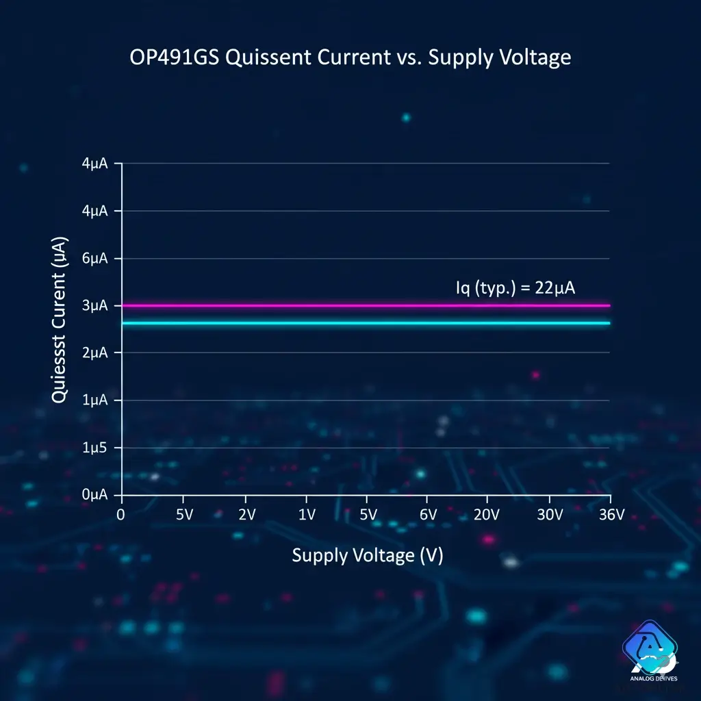
- Micropower Consumption: This is its main selling point. The OP491GS draws a typical quiescent current (Iq) of only 10 µA per amplifier. That's 0.00001 Amps. This is exceptionally low, allowing a device to run for months or even years on a small battery.
- Single-Supply Operation: It's designed to work perfectly from a single power source, with a wide operating range from +2.7V to +12V. This makes it perfect for 3V, 5V, or 9V systems.
- Rail-to-Rail Output: The output voltage swing can go almost all the way to the positive supply rail (V+) and the negative supply rail (V-, or ground in a single-supply setup). This is critical in low-voltage systems for maximizing dynamic range.
- Low Offset Voltage: With a typical offset of just 0.5 mV, it's a precision device. It won't introduce significant error when amplifying very small signals, such as from a thermocouple or a strain gauge.
1.3 Understanding the "GS" Suffix: 16-Lead SOIC
In the world of components, the letters after the main part number are critical. For the OP491, the "GS" denotes the package type:
- G: This is the product grade (not specified in all datasheets, often refers to temperature range).
- S: This specifies the package, which is a 16-Lead Standard Small Outline IC (SOIC), also known as an R-16 package.
This is a standard surface-mount package, making it easy to use in modern PCB assembly processes.
2.0 OP491GS Key Technical Specifications
Let's get into the hard numbers. If you're an engineer deciding on a part, these are the specifications you care about.
2.1 Electrical Characteristics
Here is a quick-reference table of the OP491GS's most important electrical characteristics, taken from the official datasheet.
| Parameter | Condition | Typical | Max | Unit |
|---|---|---|---|---|
| Supply Voltage (VS) | +2.7 to +12 | V | ||
| Quiescent Current (Iq) | per amplifier | 10 | 20 | µA |
| Offset Voltage (VOS) | 0.5 | 1.5 | mV | |
| Input Bias Current (IB) | 1 | 5 | nA | |
| Gain Bandwidth Product (GBWP) | 0.3 | MHz | ||
| Slew Rate (SR) | 0.1 | V/µs | ||
| Common-Mode Rejection (CMRR) | 90 | dB | ||
| Output Swing (Rail-to-Rail) | RL = 10 kΩ | (V-) + 30mV, (V+) - 200mV |
2.2 Performance: Rail-to-Rail Output Explained
The rail-to-rail output is a feature you can't overlook. Let's use an analogy.
Imagine your power supply is a 3-volt battery. Your signal is a small 0.1V sine wave from a sensor.
- A standard op-amp might only be able to swing its output between 0.5V and 2.5V. It can't get "all the way" to 0V (ground) or 3V (the rail).
- The OP491GS can swing its output from 0.03V to 2.8V.
This gives you a much larger output range to work with, which is critical for maintaining signal fidelity when your entire power source is only 3 volts.
2.3 OP491GS vs. LM324: A Comparison
Why wouldn't you just use the ultra-common, ultra-cheap LM324 quad op-amp? The answer is power and precision.
"Choosing an op-amp is a game of trade-offs. The LM324 is a low-cost, general-purpose workhorse. The OP491GS is a precision, low-power specialist."
Here’s a head-to-head comparison for a battery-powered design:
| Feature | OP491GS (Specialist) | LM324 (Generalist) |
|---|---|---|
| Quiescent Current (per amp) | 10 µA (Typical) | 700 µA (Typical) |
| Minimum Supply Voltage | 2.7 V | 3.0 V |
| Offset Voltage (VOS) | 0.5 mV (Typical) | 2.0 mV (Typical) |
| Output Swing (Single 5V Supply) | 0.03V to 4.8V (Rail-to-Rail) | 0.02V to 3.5V (Not RRO) |
| Gain Bandwidth Product | 0.3 MHz | 1.0 MHz |
The verdict is clear: The LM324 consumes 70 times more power and has 4 times the error (offset voltage). For any battery-powered design, the IC OP491GS is the obvious high-performance choice.
3.0 OP491GS Pinout and Package Details
Correctly wiring the chip is the first step to a working design. The OP491GS uses a standard 16-lead SOIC package.
3.1 16-Lead SOIC (R-16) Package Diagram
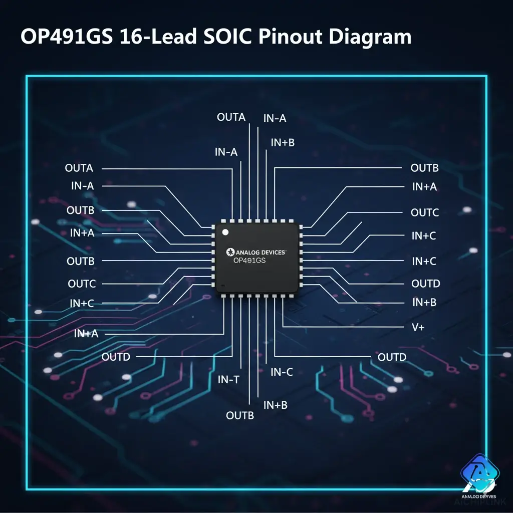
3.2 Detailed Pin Configuration
The 16 pins are logically laid out to provide access to all four independent op-amps.
| Pin | Name | Function |
|---|---|---|
| 1 | OUT A | Output of Amplifier A |
| 2 | IN A- | Inverting Input of Amplifier A |
| 3 | IN A+ | Non-Inverting Input of Amplifier A |
| 4 | V+ | Positive Power Supply |
| 5 | IN B+ | Non-Inverting Input of Amplifier B |
| 6 | IN B- | Inverting Input of Amplifier B |
| 7 | OUT B | Output of Amplifier B |
| 8 | OUT C | Output of Amplifier C |
| 9 | IN C- | Inverting Input of Amplifier C |
| 10 | IN C+ | Non-Inverting Input of Amplifier C |
| 11 | V- | Negative Power Supply (GND) |
| 12 | IN D+ | Non-Inverting Input of Amplifier D |
| 13 | IN D- | Inverting Input of Amplifier D |
| 14 | OUT D | Output of Amplifier D |
| 15 | NC | No Connect (Leave floating) |
| 16 | NC | No Connect (Leave floating) |
4.0 OP491GS Applications and Design
With its unique combination of features, the OP491GS is the perfect choice for a specific set of applications.
4.1 Common Applications (Battery-Powered, etc.)
* **Battery-Powered Instrumentation:** Think handheld gas detectors, portable light meters, or wireless weather stations. * **Portable Medical Devices:** Critical for devices like glucose meters, heart rate monitors, and oximeters where battery life and precision are essential. * **Sensor Signal Conditioning:** Buffering and amplifying signals from high-impedance sensors (like pH probes or photodiodes). * **Micropower Active Filters:** Creating low-pass or band-pass filters for audio or sensor signals without draining the battery. * **IoT Devices:** Any remote "node" that needs to wake up, take a measurement, and go back to sleep.4.2 Design Example: A Micropower Buffer Circuit
One of the most common uses for an op-amp is a **unity-gain buffer**, which is used to isolate a high-impedance source from a low-impedance load. This is especially important for sensors.Here's how you'd configure one of the four amps (e.g., Amp A) as a buffer:
- Power: Connect Pin 4 (V+) to your battery (e.g., +3.3V) and Pin 11 (V-) to Ground.
- Bypass: Place a 0.1µF ceramic capacitor directly between Pin 4 and Pin 11, as close to the IC as possible. This is critical for stability.
- Input: Connect your sensor's signal to the non-inverting input, Pin 3 (IN A+).
- Feedback: Connect the output, Pin 1 (OUT A), directly back to the inverting input, Pin 2 (IN A-).
- Output: Your buffered signal is now available at Pin 1.
This simple circuit will draw only 10µA from your supply but will provide a robust, low-impedance output that can drive the next stage of your circuit, like an ADC.
4.3 Finding an OP491GS Replacement or Equivalent
If you have a design that uses the **IC OP491GS** and you can't find one, you need to look for a replacement that matches its key specs: * **Package:** 16-Lead SOIC * **Pinout:** Must be identical (many quad op-amps share this standard pinout) * **Key Specs:** Micropower (Iq < 20µA/amp), single-supply (works at 3V), and rail-to-rail output. A potential replacement might be the **TLC27L4** or **MCP6004**, but you **must** check the pinout and specifications carefully before swapping. For a guaranteed, drop-in replacement, you should source the original **OP491GS** from a reliable distributor.In Conclusion
The IC OP491GS Quad Operational Amplifier is not your everyday, general-purpose op-amp. It is a precision specialist designed for one of the most challenging areas of modern electronics: battery-powered design. By offering four reliable, high-precision amplifiers in a single package that sips a mere 10µA of current per channel, it provides the perfect solution for portable instrumentation.
As the world continues to move toward smaller, more efficient, and longer-lasting portable and IoT devices, the principles of micropower design embodied by the OP491GS will only become more critical.
If your design demands low power without sacrificing precision, the OP491GS is a top-tier choice. For this and other high-performance analog components, browse our full range of operational amplifiers to find the perfect part for your next project.

Written by Jack Elliott from AIChipLink.
AIChipLink, one of the fastest-growing global independent electronic components distributors in the world, offers millions of products from thousands of manufacturers, and many of our in-stock parts is available to ship same day.
We mainly source and distribute integrated circuit (IC) products of brands such as Broadcom, Microchip, Texas Instruments, Infineon, NXP, Analog Devices, Qualcomm, Intel, etc., which are widely used in communication & network, telecom, industrial control, new energy and automotive electronics.
Empowered by AI, Linked to the Future. Get started on AIChipLink.com and submit your RFQ online today!
Frequently Asked Questions
What is the OP491GS used for?
The OP491GS is a quad micropower operational amplifier used in battery-powered applications where low power consumption is critical. Common uses include portable medical instruments, sensor signal conditioning, and low-power active filters.
What is the supply voltage for the OP491GS?
The OP491GS is designed for single-supply operation from **+2.7V to +12V**, or dual-supply operation from ±1.35V to ±6V. Its key feature is its ability to run on very low voltage and power.
Is the OP491GS a rail-to-rail op-amp?
The OP491GS features a **rail-to-rail *output*** stage. This means its output voltage can swing very close to the positive (V+) and negative (V-) supply rails, maximizing the dynamic range in low-voltage, single-supply systems. Its input range is not rail-to-rail.
What is the difference between the OP491GS and the LM324?
The main difference is power and precision. The OP491GS consumes about 70 times less power (10µA vs 700µA per amp) and has 4 times lower offset voltage (0.5mV vs 2mV). The OP491GS is a high-precision, low-power specialist, while the LM324 is a low-cost, general-purpose part. For more on the classic LM324, check out its **<u><a href="https://en.wikipedia.org/wiki/LM324" target="_blank">Wikipedia page</a></u>**.
What does "micropower" mean for an op-amp?
"Micropower" is a term for components that consume extremely low quiescent current (Iq), typically in the microamp (µA) range. This makes them ideal for extending the battery life of portable and "always-on" sensing devices.