Introduction
Every precision analog engineer eventually faces the same frustrating power design problem: the system runs on a single 3.3 V or 5 V USB or battery supply, but the op-amp datasheet requires ±5 V, the audio DAC needs ±2.5 V, or the RF power amplifier gate bias demands −3 V. Generating a negative supply rail from a positive input is notoriously awkward — charge pumps based on the MAX1044 vintage topology are noisy and limited in current, inverting buck-boost converters are complex and EMI-intensive, and dedicated negative LDOs require an external negative voltage source that doesn't exist in a single-supply system.
The LM27762DSSR from Texas Instruments elegantly resolves this problem. By integrating an inverting switched-capacitor charge pump (operating at 2 MHz to minimize ripple) followed by a low-noise negative LDO, alongside a second low-noise positive LDO fed directly from the input, the LM27762 generates independently adjustable positive and negative output voltages between ±1.5 V and ±5 V — both rails simultaneously, from a single 2.7 V to 5.5 V supply — with just five external capacitors and four resistors, consuming only 390 µA of operating quiescent current.
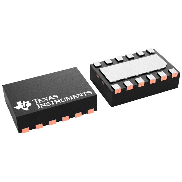
According to TI's Precision Analog Design Center, the combination of charge pump noise and LDO filtering is the most effective single-chip architecture for generating low-noise bipolar rails in the 100–250 mA current range — the LDO stage suppresses the inherent switching ripple of the charge pump before it reaches the load, delivering output noise performance comparable to a purely linear LDO while eliminating the need for a separate negative input supply. The LM27762DSSR is the production implementation of this architecture in the most common ordering format: 12-pin WSON (3 mm × 2 mm), tape-and-reel.
1.0 What Is the LM27762DSSR? An Overview
The LM27762DSSR is a fully integrated, dual-rail, positive and negative output power management IC from Texas Instruments. It simultaneously generates one positive and one negative regulated output voltage from a single low-voltage positive supply — a complete bipolar supply solution in a single chip measuring just 3 mm × 2 mm.
Decoding the ordering code:
- LM27762 — Product family: low-noise dual-rail charge pump + LDO power management IC
- D — Dual-output, adjustable variant (positive and negative outputs both set by external R1–R4 resistors)
- SS — 12-pin WSON package (3 mm × 2 mm body, exposed thermal/ground pad)
- R — Tape-and-reel packaging (2,500 pcs/reel standard)
The companion ordering code LM27762DSST is the same IC in bulk tray packaging — electrically identical. The package code "SS" designates the 12-pin WSON (3×2 mm) with exposed pad — TI's standard small form factor for this level of pin count.
"The LM27762 delivers very low-noise positive and negative outputs that are adjustable between ±1.5 V and ±5 V. Input voltage range is from 2.7 V to 5.5 V, and output current goes up to ±250 mA. With an operating current of only 390 µA and 0.5-µA typical shutdown current, the LM27762 provides ideal performance for power amplifier and DAC bias and other high-current, low-noise negative voltage needs." — Texas Instruments LM27762 Datasheet, Rev. C
The LM27762 is the evolution of TI's LM27761 (which provided only a negative output). The LM27762 adds a complete second LDO for a regulated positive output from the same input rail — making it a true one-chip bipolar supply solution rather than a negative-only accessory.
2.0 Full Technical Specifications & Dual-Rail Architecture
2.1 Core Electrical Parameters
The following parameters are from the LM27762 datasheet (Rev. C), at VIN = 5 V, VOUT+ = 2.5 V, VOUT− = −2.5 V, TA = 25°C, unless noted:
- Input Voltage Range (VIN): 2.7 V to 5.5 V
- Positive Output Voltage Range (VOUT+): +1.5 V to +5.0 V (adjustable via R1/R2)
- Negative Output Voltage Range (VOUT−): −1.5 V to −5.0 V (adjustable via R3/R4)
- Maximum Output Current (each rail): ±250 mA
- Positive LDO Dropout Voltage: ~200 mV at 250 mA (typical)
- Negative LDO Dropout Voltage: ~30 mV at 100 mA (very low due to PMOS architecture)
- Charge Pump Switching Frequency: 2 MHz typical (1.7–2.3 MHz range)
- Positive Internal Reference (VFB+): ~0.5 V (sets VOUT+ via R1/R2 divider)
- Negative Internal Reference (VFB−): ~0.5 V (sets VOUT− magnitude via R3/R4)
- Feedback Resistor Minimum (R2, R4): ≥ 50 kΩ (required for regulator stability)
- Operating Quiescent Current (IQ): 390 µA typical (both rails active, no load)
- Shutdown Current (ISHDN): 0.5 µA typical (EN+ and EN− both low)
- Enable Inputs (EN+, EN−): Independent, active-high, CMOS-compatible; supports individual rail sequencing
- Power Good (PGOOD): Optional open-drain output; asserts when both rails are within regulation (pull-up resistor required)
- Thermal Shutdown (TSD): Yes — activates at ~150°C junction temperature
- Operating Temperature Range: −40°C to +85°C
- Package: 12-pin WSON, 3 mm × 2 mm body, 0.5 mm lead pitch, exposed thermal pad (EP)
- Flying Capacitor (C1): External, between C1+ and C1− pins; recommended 1 µF X5R ceramic
- Required External Capacitors: 5 total (CIN, C1, COUT+, COUT−, and one additional for charge pump)
- MSL Rating: MSL 3
- RoHS Compliant: Yes (Pb-free)
- ECCN: EAR99
- Evaluation Module: LM27762EVM
2.2 Inverting Charge Pump + Negative LDO Architecture
The LM27762's dual-rail generation uses two fundamentally different power conversion topologies in a single package:
Positive rail (VOUT+): Implemented as a standard linear dropout (LDO) regulator — the input rail (VIN) passes through a PMOS pass transistor whose gate is controlled by an error amplifier comparing a VIN-referenced feedback voltage to an internal reference. The result is a low-noise, stable positive output with PSRR dominated by the LDO's loop gain. No switching, no external inductors, no radiated EMI from the positive path.
Negative rail (VOUT−): Implemented as a two-stage converter — first an inverting switched-capacitor charge pump, then a negative LDO post-regulator:
Stage 1 — Inverting Charge Pump: Four large internal CMOS switches alternate between two phases at 2 MHz:
- Phase 1 (Charge): S1 and S3 close; the flying capacitor C1 charges to approximately +VIN through the internal switches
- Phase 2 (Invert): S2 and S4 close; the flying capacitor is connected with reversed polarity, delivering approximately −VIN to the intermediate charge pump output node
The charge pump generates an intermediate voltage of approximately −VIN (before LDO regulation). The 2 MHz switching frequency minimizes the charge pump's output impedance and reduces ripple voltage on the charge pump output — directly improving the negative LDO's input quality.
Stage 2 — Negative LDO: The charge pump output (approximately −VIN) feeds a negative-input LDO that regulates the final VOUT− to the desired level (−1.5 V to −5.0 V). This LDO stage provides:
- Ripple rejection: Attenuates the 2 MHz charge pump switching ripple before it reaches the load
- Output noise reduction: The LDO's error amplifier loop bandwidth suppresses wideband noise from the charge pump
- Tight regulation: The VOUT− is regulated to within ±2% of the target despite load current and input voltage variations
- Ultra-low dropout: ~30 mV at 100 mA on the negative side — the LDO has very little overhead to lose before dropping out
This two-stage architecture is why the LM27762 can claim "low-noise" for its negative output despite the charge pump stage: the LDO post-regulator does the heavy lifting of noise filtering, achieving noise performance comparable to a purely linear supply.
2.3 Headroom Requirements, Dropout, and Operating Limits
Designing with the LM27762 requires understanding the cascade headroom needed by the charge pump and LDO combination. Unlike a simple LDO where VIN − VOUT ≥ VDO is the only constraint, the LM27762 negative rail has a two-stage headroom budget:
Positive rail headroom: VIN − VOUT+ ≥ VDO_POS ≈ 200 mV at 250 mA
For VOUT+ = 3.3 V, minimum VIN = 3.5 V — easily met with a 3.6 V or 5 V supply. For VOUT+ = 5.0 V from VIN = 5.0 V, the positive LDO is in deep dropout — reduce VOUT+ or increase VIN.
Negative rail headroom (the more critical constraint):
|VOUT−| ≤ |VCP_output| − VDO_NEG
where VCP_output ≈ VIN − R_CP × I_LOAD_NEG
The charge pump output resistance (R_CP) is a function of the flying capacitor value and the switching frequency. With C1 = 1 µF and fSW = 2 MHz: R_CP ≈ 1/(2 × fSW × C1) = 1/(2 × 2M × 1µ) = 0.25 Ω. At IOUT− = 250 mA: VCP_output ≈ VIN − 0.25 × 0.25 = VIN − 0.0625 V. This is negligible — the charge pump's output resistance is very low at 2 MHz with a 1 µF flying capacitor.
Practical operating envelope summary:
| VIN | Max |VOUT+| | Max |VOUT−| | Notes | |---|---|---|---| | 2.7 V | 2.5 V | 2.5 V | Minimum supply for LM27762 | | 3.3 V | 3.1 V | 3.1 V | Single-cell Li-Ion, USB2.0 low supply | | 5.0 V | 4.8 V | 4.8 V | USB 5 V / regulated 5 V supply | | 5.5 V | 5.0 V (limit) | 5.0 V (limit) | Maximum input; near-maximum output |
Note that VOUT+ = VIN − VDO is the positive rail limit, and |VOUT−| ≤ |VIN − VDO_CP_total| is the negative rail limit. Attempting to set VOUT+ or |VOUT−| beyond these limits causes the LDO to drop out and the output to follow input rather than regulation.
2.4 Light-Load Burst Mode and 2 MHz Continuous Mode
The LM27762's charge pump operates in two distinct modes depending on load current:
Continuous (CCM) mode at loads > ~107 mA (negative rail): The charge pump runs at a fixed 2 MHz switching frequency. Output resistance is minimized, ripple is at the charge pump fundamental frequency (2 MHz), and the negative LDO post-regulator presents a clean, well-regulated output. This is the normal high-load operating condition for audio, RF PA bias, and op-amp supply applications.
Burst (DCM / discontinuous) mode at light loads < ~107 mA: At low load currents, the charge pump does not need to switch continuously to maintain the output voltage. The internal controller enters burst mode — switching in short bursts and then pausing — to reduce switching losses and improve light-load efficiency. During burst mode, the charge pump's effective switching frequency drops from 2 MHz to as low as a few kilohertz, which shifts the ripple energy to lower frequencies.
Design implication: In audio applications or RF circuits where low-frequency spurious tones are particularly damaging (they fall within the audio passband or inside the RF channel bandwidth), light-load burst mode can be problematic. The negative LDO post-regulator attenuates this burst-mode ripple significantly, but some residual low-frequency ripple may be visible at very light loads (< 10 mA). Solutions:
- Add a minimum load resistor (100–500 Ω from VOUT− to GND) to keep the load above the CCM threshold during idle periods
- Use the negative LDO's PSRR to rely on additional attenuation of the burst-mode ripple
- Add a post-filter (small ferrite bead + 10 µF ceramic) between VOUT− and the noise-sensitive load for extra isolation
In most practical applications (op-amp supply drawing > 10 mA, audio DAC at moderate volume), the system naturally stays above the burst mode threshold and operates cleanly in continuous mode.
3.0 Output Voltage Design and Application Circuits
3.1 R1–R4 Output Voltage Setting: Formulas and Design Tables
The LM27762DSSR uses two independent resistor dividers — R1/R2 for the positive output and R3/R4 for the negative output — to set the two regulated output voltages:
Positive output (VOUT+): VOUT+ = VFB+ × (1 + R1/R2)
where VFB+ is the internal reference voltage at the FB+ pin (refer to the LM27762 datasheet for the exact VFB+ value at your operating conditions — approximately 0.5 V typical, but verify from the electrical specifications table).
Constraint: R2 ≥ 50 kΩ (minimum; required for regulator stability and to avoid excessive reference loading).
Negative output (VOUT−): |VOUT−| = VFB− × (1 + R3/R4)
where VFB− is the internal reference voltage at the FB− pin (same magnitude as VFB+, approximately 0.5 V typical). The negative output voltage magnitude is set the same way as the positive, but the actual output is the negative of the computed value.
Constraint: R4 ≥ 50 kΩ (same requirement as R2).
Practical design procedure:
- Choose R2 = R4 = 100 kΩ (well above 50 kΩ minimum; keeps divider current reasonable)
- Calculate R1 = R2 × (|VOUT+| / VFB+ − 1) and R3 = R4 × (|VOUT−| / VFB− − 1)
- Select nearest E96 standard 1% resistor values
- Use TI's WEBENCH Power Designer or LM27762EVM TINA-TI simulation to verify
Common output voltage configurations (R2 = R4 = 100 kΩ, VFB ≈ 0.5 V):
| ±VOUT Target | R1 (= R3) calculated | R1 (E96 nearest) | Actual ±VOUT |
|---|---|---|---|
| ±1.5 V | 200 kΩ | 200 kΩ | ±1.5 V |
| ±1.8 V | 260 kΩ | 261 kΩ | ±1.805 V |
| ±2.5 V | 400 kΩ | 402 kΩ | ±2.51 V |
| ±3.3 V | 560 kΩ | 562 kΩ | ±3.31 V |
| ±5.0 V | 900 kΩ | 909 kΩ | ±5.045 V |
Note: Exact VFB values should be taken from the LM27762 datasheet electrical characteristics table for your operating temperature. The above assumes VFB = 0.5 V for illustration. Asymmetric positive and negative voltages are fully supported — simply choose different R1/R2 and R3/R4 ratios independently.
Asymmetric supply example (VOUT+ = +3.3 V, VOUT− = −2.5 V): Set R1/R2 for 3.3 V and R3/R4 for 2.5 V independently. This is a common requirement for mixed-signal circuits where the positive rail powers digital logic (3.3 V) and the negative rail biases a bipolar op-amp or DAC at a lower magnitude.
3.2 Independent EN+/EN− and Power-Good Sequencing
The LM27762DSSR provides separate enable pins for the positive and negative rails:
- EN+: Enables the positive LDO. When low (or floating, since there is no internal pulldown — tie EN+ to VIN for always-on operation), the positive rail is off.
- EN−: Enables the negative charge pump and LDO. When low, the negative rail is off. EN+ and EN− can be tied together to a single control signal for simultaneous enable/disable.
Sequencing capability: The independent enables allow the positive rail to be brought up before the negative rail (or vice versa) — critical in systems where the op-amp or IC powered by the bipolar supply has specific power-up sequence requirements. For example, many precision op-amps specify that the positive supply must be applied before or simultaneously with the negative supply to avoid latch-up. With LM27762, simply delay EN− relative to EN+ using an RC delay circuit on the EN− pin.
Power Good (PGOOD): An optional open-drain output that requires an external pull-up resistor (typically 100 kΩ to VIN or a logic supply). PGOOD asserts HIGH when both VOUT+ and VOUT− are within regulation. It goes LOW during startup, fault conditions, or when either rail is out of regulation. Connect PGOOD to a microcontroller GPIO or a downstream enable input to implement supervised power sequencing: the MCU waits for PGOOD to assert before initializing analog peripherals, preventing spurious analog circuit behavior during the LM27762's startup ramp.
3.3 Precision Op-Amp, DAC, and Analog Circuit Bipolar Supply
The LM27762DSSR was explicitly designed by TI for precision analog circuit supply — specifically the applications where a single-supply system needs a clean, regulated bipolar rail for:
Precision instrumentation amplifiers and op-amps: Devices like the TI INA128, OPA2134, or AD8676 are specified for ±5 V or ±15 V operation and require a clean bipolar supply. Running from LM27762's ±5 V maximum (from a 5.5 V input) covers the ±5 V supply requirement. The LM27762's low output noise (enabled by the LDO post-regulator on the negative rail) prevents noise from the power supply from coupling into the op-amp's power supply rejection path and appearing as output noise.
High-resolution DACs (16–24 bit): Audio DACs and precision measurement DACs require a stable, low-noise bipolar supply for their internal reference and output stage. Supply noise coupling through the DAC's PSRR can manifest as spectral spurs in the DAC output spectrum. The LM27762's negative rail LDO suppresses the 2 MHz charge pump switching frequency and its harmonics, keeping the DAC's output spectrum clean. For a 24-bit DAC with 120 dB dynamic range, power supply noise must be < 10 µV RMS in the audio band — achievable with the LM27762 + adequate COUT− filtering.
Signal conditioning circuits (MUX, sample-and-hold, precision comparators): Circuits that must process bipolar analog signals (−2.5 V to +2.5 V) require a bipolar supply to avoid clipping. The LM27762DSSR provides both supply rails from a single 5 V USB power source, eliminating the need for a separate negative voltage input — a fundamental BOM simplification for portable instruments.
3.4 Audio Headphone Amplifier and RF PA Bias Applications
Audio headphone amplifier: USB-powered portable headphone amplifiers typically run from 5 V USB, yet the headphone driver op-amp (e.g., OPA1622, LME49600) benefits from a ±5 V bipolar supply that allows a wider output voltage swing (and thus lower distortion at high output levels). The LM27762DSSR generates ±5 V from 5 V USB directly — the positive LDO outputs +5 V with ~200 mV headroom from the 5.5 V regulated input (or use a small boost to 5.5 V), and the negative rail delivers −5 V via the charge pump + LDO path. Both rails are available at 250 mA — sufficient for dual-channel headphone output driving 32–300 Ω headphone loads.
RF power amplifier gate bias: GaAs pHEMT and GaN power amplifiers require a negative gate bias voltage (typically −0.5 V to −3.5 V) to set the operating point. The bias supply must be:
- Low noise — gate voltage noise modulates the PA's transconductance, degrading ACPR and EVM in the RF output
- Stable under temperature — the PA's quiescent current varies with temperature; a well-regulated bias prevents thermal runaway
- Available from positive input — PA modules typically have only a positive drain supply input
The LM27762DSSR provides all three: low noise (LDO post-regulator on negative rail), ±2% voltage accuracy over temperature, and negative rail generation from a positive 3.3 V or 5 V input. The EN− pin allows the gate bias to be applied after the drain supply (EN−-delay sequencing), preventing PA device damage during power-up.
4.0 LM27762DSSR vs. Competing Bipolar Supply ICs
4.1 LM27762DSSR vs. TPS65133, LM27761, MAX1044, and TPS7A39
| Feature | LM27762DSSR | TPS65133 | LM27761DCKR | MAX1044 | TPS7A39DSSR |
|---|---|---|---|---|---|
| Architecture | CP + LDO (+ LDO) | CP + LDO (+ LDO) | CP + LDO (neg only) | Unregulated CP | Dual LDO (no CP) |
| Positive Rail | Yes (LDO, adjustable) | Yes (LDO) | No | No | Yes (LDO, adj.) |
| Negative Rail | Yes (CP+LDO, adjustable) | Yes (CP+LDO) | Yes (CP+LDO, adj.) | Yes (unregulated) | Yes (LDO, adj.) |
| VIN Range | 2.7–5.5 V | 2.7–5.5 V | 2.7–5.5 V | 1.5–10 V | 2.9–5.5 V |
| Max IOUT+ / IOUT− | ±250 mA | ±150 mA | 0 / 250 mA | 0 / 10–40 mA | ±300 mA |
| Charge Pump Freq. | 2 MHz | 2 MHz | 2 MHz | ~10–50 kHz | N/A |
| Output Voltage Range | ±1.5 to ±5.0 V | ±1.5 to ±5.5 V | −1.5 to −5 V | ~−VIN (unreg.) | −0.8 to −5.5 V |
| Regulated Negative? | Yes (LDO) | Yes (LDO) | Yes (LDO) | No | Yes (LDO) |
| Operating IQ | 390 µA | ~360 µA | ~200 µA | ~100 µA | ~300 µA |
| Output Accuracy | ±2% | ±2% | ±2% | ±10–15% (unregulated) | ±2% |
| Independent EN+/EN− | Yes | No (single EN) | No (single EN) | No | Yes |
| Power Good | Yes (PGOOD) | No | No | No | Yes (PGOOD) |
| Package | WSON-12 (3×2mm) | WSON-12 (3×2mm) | SOT-23-8 (3×3mm) | DIP-8 / SO-8 | WSON-12 (3×2mm) |
| Price/Unit (1k) | ~$1.10–$1.60 | ~$1.30–$1.80 | ~$0.60–$0.90 | ~$0.40–$0.80 | ~$1.30–$1.80 |
Key selection guidance:
- Need ±250 mA bipolar, adjustable ±1.5 to ±5 V, independent sequencing, PGOOD → LM27762DSSR — this device; the most feature-complete integrated bipolar supply in its class, with independent EN+/EN− for sequencing and PGOOD for supervised startup
- Need lower cost, ±150 mA sufficient, no independent sequencing needed → TPS65133 — similar architecture, lower maximum current, single EN pin, slightly lower price
- Need negative rail only (positive rail from a separate regulator) → LM27761DCKR — negative-only version of the LM27762 concept; smaller 8-pin SOT-23 package, lower cost when positive rail is already available
- Need very low cost, basic voltage inversion without regulation → MAX1044 — unregulated charge pump inverter; output tracks −VIN, no LDO regulation, very low current (~10–40 mA); acceptable only for analog circuits with their own inherent ripple rejection (bypassed op-amp references) at much lower cost
- Need ±300 mA bipolar from a single 2.9–5.5 V supply using LDOs only (no charge pump noise concerns) → TPS7A39DSSR — TI's dual-rail LDO alternative; requires the external voltage to already have both polarities (or uses a bootstrapped negative-rail scheme); higher current but different input architecture
4.2 Ordering Codes, Package Options & Availability {#compare-source}
LM27762 ordering code decoder:
- LM27762DSSR — Adjustable, WSON-12 (3×2 mm), tape-and-reel, 2,500 pcs/reel (this article's subject)
- LM27762DSST — Adjustable, WSON-12 (3×2 mm), bulk tray — same device, tray packaging for prototyping/hand assembly
Fixed-output variants (internal resistors, no external R1–R4 required) use a different suffix structure — consult TI's product page for available fixed voltages (e.g., ±1.8 V, ±2.5 V, ±5.0 V).
Availability and pricing:
- Authorized distributors: DigiKey, Mouser, Arrow, Avnet, LCSC
- Typical unit pricing: ~$1.10–$1.60 USD (1k+ quantity tape-and-reel)
- LCSC pricing: as low as ~$0.46 USD for single units (verify authenticity)
- Lead time: Generally in-stock at DigiKey and Mouser; 8–14 week standard lead time during supply-constrained periods
- RoHS status: Fully compliant (Pb-free termination)
- ECCN: EAR99
- Evaluation module: LM27762EVM (~$49 USD from TI) — pre-populated WSON-12 evaluation board with SMAs for all inputs/outputs, test points, onboard pull-up resistors for PGOOD, and header-accessible EN+/EN−
For verified authentic TI inventory, competitive pricing, and volume RFQ support, visit aichiplink.com — LM27762DSSR listing.
5.0 PCB Layout and Design Optimization
5.1 Flying Capacitor, CIN, COUT+ and COUT− Placement
Capacitor placement is the single most critical PCB layout consideration for the LM27762DSSR. TI's datasheet layout note is direct: connections using long trace lengths, narrow trace widths, or vias must be avoided for the flying capacitor and output capacitors — these add parasitic inductance and resistance that degrades performance, especially during transients.
Flying capacitor (C1): Connects between the C1+ and C1− pins. This capacitor transfers charge on every switching cycle — the trace inductance between C1 and its pins directly adds to the effective charge pump output impedance, increasing output ripple and reducing current delivery capability. Use 1 µF X5R ceramic, 0402 size, placed as close to the C1+ and C1− pins as physically possible. Route the C1+ and C1− traces as short, wide (≥ 0.5 mm) traces on the same PCB layer as the IC, with the C1 capacitor body spanning across the gap between the two pins.
CIN (Input capacitor): Place a 2.2 µF X5R ceramic at the VIN pin, return path to the exposed pad (GND). CIN must supply the charge pump's switching current transients — inadequate CIN causes VIN to droop during charge pump switching, which can cause oscillation in an upstream regulator (a well-documented real-world issue: the LM27762's 2 MHz charge pump presents a negative incremental impedance to the input, which can destabilize upstream low-bandwidth LDOs). TI recommends ensuring the upstream supply source impedance is low at 2 MHz — either use a stiff upstream regulator (high bandwidth), or place a 4.7 µF bulk capacitor at the LM27762 VIN pin to decouple the charge pump current from the upstream supply's output impedance.
COUT+ (Positive output capacitor): Place a 2.2 µF X5R ceramic at the OUT+ pin, directly returned to the exposed pad GND. Minimum 1 µF for stability; 2.2 µF recommended for improved transient response.
COUT− (Negative output capacitor): Place a 2.2 µF X5R ceramic at the OUT− pin, directly returned to GND. Same size and placement requirements as COUT+. The negative rail COUT is particularly important for suppressing burst-mode low-frequency ripple at light loads.
Recommended capacitor type for all five positions: X5R or X7R ceramic, rated at ≥ 2× the operating voltage. Avoid Y5V or Z5U dielectrics — their severe capacitance derating with DC bias means a nominal 2.2 µF Y5V at operating voltage may provide < 0.5 µF effective capacitance, causing instability and poor transient performance.
5.2 WSON-12 Package, Exposed Pad, and Ground Topology
The 12-pin WSON (3 mm × 2 mm) package has leads on a 0.5 mm pitch and a central exposed pad (EP). TI's datasheet layout guidance emphasizes a key requirement: all ground connections must be on the top layer and should connect back to the LM27762's exposed pad directly, avoiding vias to inner ground planes for the local IC ground.
This guidance is motivated by the LM27762's unique ground structure — both the positive LDO and the negative charge pump/LDO share a single ground pin (GND/EP). Any inductance in the ground path between the IC's EP and the reference point for the capacitor returns creates a common-mode feedback path that can cause oscillation or increased ripple.
Practical layout rules:
- Solid exposed pad solder: The EP must be fully soldered to a top-layer ground copper area. Place 4 small (0.2 mm drill) thermal vias in the EP pad, but keep via inductance low by ensuring they connect to a large copper area on the top layer that physically connects to all five capacitor returns.
- Star ground on top layer: Route all five capacitor return terminals (GND side of CIN, C1, COUT+, COUT−) directly to the EP ground copper on the top layer, forming a local star ground around the IC. Avoid routing capacitor returns through vias to inner layers and back — this adds inductance that degrades the charge pump's ripple performance.
- Feedback resistors (R1–R4): Place all four resistors on the top layer, adjacent to the FB+ and FB− pins respectively. The ground return of R2 and R4 must connect to the EP ground directly — do not route through long traces to a distant ground via.
- Keep-away from digital switching signals: Route the LM27762 and its capacitors away from high-frequency digital switching signals (MCU clock lines, DCDC switching nodes) to prevent noise coupling into the sensitive feedback network.
5.3 Input Supply Decoupling and Upstream Regulator Interaction
A significant practical challenge with the LM27762DSSR — documented in both TI's application notes and in community engineering forums — is the interaction between the LM27762's 2 MHz charge pump and an upstream linear regulator or LDO. The charge pump's switched-capacitor operation presents a negative incremental input impedance at the switching frequency, which can cause oscillation if the upstream source impedance is not sufficiently low at 2 MHz.
Root cause: When the charge pump switches, it draws current pulses from VIN at 2 MHz. An upstream LDO with limited bandwidth (typically 100 kHz–1 MHz loop bandwidth) cannot regulate its output fast enough to absorb these pulses, causing VIN to oscillate. The 2 MHz pulses modulate the LDO's error amplifier, creating a feedback loop with negative phase margin.
Solutions:
- Large local input capacitor: The most reliable solution is to place a 10 µF + 2.2 µF ceramic capacitor combination directly at the LM27762's VIN pin, with returns going to EP GND on the top layer. This bulk capacitance absorbs the 2 MHz current pulses locally, isolating the upstream LDO from the charge pump transients.
- Use a stiff, high-bandwidth upstream supply: A well-designed DCDC buck converter (typically > 500 kHz bandwidth) with adequate output capacitance can tolerate the LM27762's pulsed load without oscillation. Low-bandwidth LDOs (e.g., LP5907) with limited loop bandwidth may oscillate when driving the LM27762 directly without sufficient local decoupling.
- Add an LC filter between upstream supply and LM27762 VIN: A small ferrite bead (100 Ω @ 2 MHz, ≥ 500 mA rating) + 4.7 µF ceramic capacitor acts as a 2 MHz low-pass filter, isolating the upstream supply from the charge pump switching current while maintaining DC voltage delivery.
- Minimum load on upstream supply: Ensuring the upstream LDO always has a DC minimum load (≥ 10 mA through a parallel resistor) maintains the LDO in its linear operating region and improves its stability margin when the LM27762 is attached.
6.0 How to Source Authentic LM27762DSSR Units
The LM27762DSSR's relatively modest pricing (~$1.10–$1.60 at volume) and wide use in audio and precision analog equipment have attracted secondary market counterfeiting. A counterfeit LM27762DSSR may generate bipolar voltages approximately but with incorrect noise performance (missing or degraded LDO post-regulator on the negative rail), incorrect switching frequency (wrong charge pump capacitor values), higher IQ, or failure to meet the ±2% output accuracy specification over temperature.
In an audio headphone amplifier, a counterfeit LM27762 with degraded negative rail LDO performance might increase the noise floor by 10–20 dBV — clearly audible as hiss in high-impedance headphones. In a precision ADC supply, incorrect voltage accuracy can shift the ADC's reference voltage, introducing a gain error that affects every measurement in the system.
Sourcing guidelines:
- Purchase from TI authorized distributors only: DigiKey, Mouser, Arrow, Avnet are Texas Instruments' authorized stocking distributors for the LM27762DSSR. These channels guarantee genuine TI silicon with full traceability.
- Verify WSON-12 package marking: The LM27762DSSR's 3 mm × 2 mm body carries a date/lot code and device identifier. At this package size, markings are tiny — inspect under 10× magnification. Characters should be sharp, laser-etched, and consistent with TI's standard package marking format.
- Functional verification: Assemble a test board with R1 = R3 = 400 kΩ, R2 = R4 = 100 kΩ (for ±2.5 V output), C1 = CIN = COUT+ = COUT− = 2.2 µF ceramic. Apply VIN = 5 V. Measure VOUT+ (should be +2.5 V ± 2% = +2.45 to +2.55 V) and VOUT− (should be −2.5 V ± 2% = −2.45 to −2.55 V). Measure IQ with no load (should be approximately 390 µA from VIN). Measure VOUT− ripple at 100 mA load on an oscilloscope — genuine LM27762 should show < 10 mV peak-to-peak ripple at the 2 MHz charge pump frequency.
- Request CoC for volume orders: For production quantities from secondary sources, require a Certificate of Conformance with TI lot traceability before acceptance.
For verified authentic Texas Instruments LM27762DSSR inventory with competitive pricing and technical support, visit aichiplink.com.
7.0 Conclusion
The LM27762DSSR solves one of analog and audio circuit design's most persistent frustrations — generating a clean, regulated bipolar supply from a single low-voltage source — with a level of integration and elegance that discrete solutions cannot match. Its 2 MHz inverting charge pump followed by a low-noise negative LDO, combined with a second low-noise positive LDO on the same die, delivers independently adjustable ±1.5 V to ±5 V at ±250 mA from a single 2.7 V to 5.5 V input, using only five external capacitors and four resistors, in a 3 mm × 2 mm WSON-12 footprint that consumes just 390 µA of quiescent current.
The independent EN+/EN− enables with power sequencing support and the optional PGOOD output give system designers the supervisory control needed for safe, ordered power-up of sensitive analog circuits. The 2 MHz switching frequency minimizes flying capacitor size while the LDO post-regulator on the negative rail ensures that switching ripple never reaches the load — making the LM27762DSSR's low-noise claim genuinely achievable in practice, not just on paper.
For engineers designing USB-powered precision instruments, portable audio DAC/amplifier systems, single-supply RF PA bias circuits, or any application requiring a low-noise bipolar rail from a positive-only source, the LM27762DSSR represents the most integrated, lowest-component-count, and most supply-efficient solution available in TI's portfolio.
Ready to design? Explore the LM27762EVM evaluation module for rapid prototyping, or source verified authentic TI inventory with competitive pricing and expert technical support at aichiplink.com — LM27762DSSR.

Written by Jack Elliott from AIChipLink.
AIChipLink, one of the fastest-growing global independent electronic components distributors in the world, offers millions of products from thousands of manufacturers, and many of our in-stock parts is available to ship same day.
We mainly source and distribute integrated circuit (IC) products of brands such as Broadcom, Microchip, Texas Instruments, Infineon, NXP, Analog Devices, Qualcomm, Intel, etc., which are widely used in communication & network, telecom, industrial control, new energy and automotive electronics.
Empowered by AI, Linked to the Future. Get started on AIChipLink.com and submit your RFQ online today!
Frequently Asked Questions
Can LM27762DSSR generate different positive and negative voltages?
Yes. The LM27762DSSR from Texas Instruments allows the positive and negative outputs to be configured independently using separate resistor dividers. Designers can set different voltages such as +3.3 V and −2.5 V as long as both outputs remain within the device’s operating limits.
Why must R2 and R4 be at least 50 kΩ?
The minimum 50 kΩ resistor value helps maintain stability in the internal LDO feedback loop. Using smaller resistors could overload the internal reference circuit, which may reduce voltage accuracy or cause instability.
What is the maximum load current for the negative output?
The LM27762DSSR supports up to 250 mA output current per rail. The positive and negative outputs are regulated independently, but both draw power from the same input supply, so the total input current must be sufficient to support both loads.
Can LM27762DSSR generate +5 V from a 5 V input?
It is possible but not ideal. Because the positive output uses an LDO stage, generating +5 V from a 5 V input leaves almost no voltage headroom, meaning the regulator may drop out under moderate load conditions.
How can oscillation in the upstream power supply be prevented?
To improve stability, designers should place a local 10 µF ceramic capacitor at the VIN pin of the LM27762DSSR and may add a ferrite bead between the upstream regulator and the device input to reduce switching noise from the internal charge pump.


.png&w=256&q=75)


