Key Components and Parameters of Flyback Converter Circuits
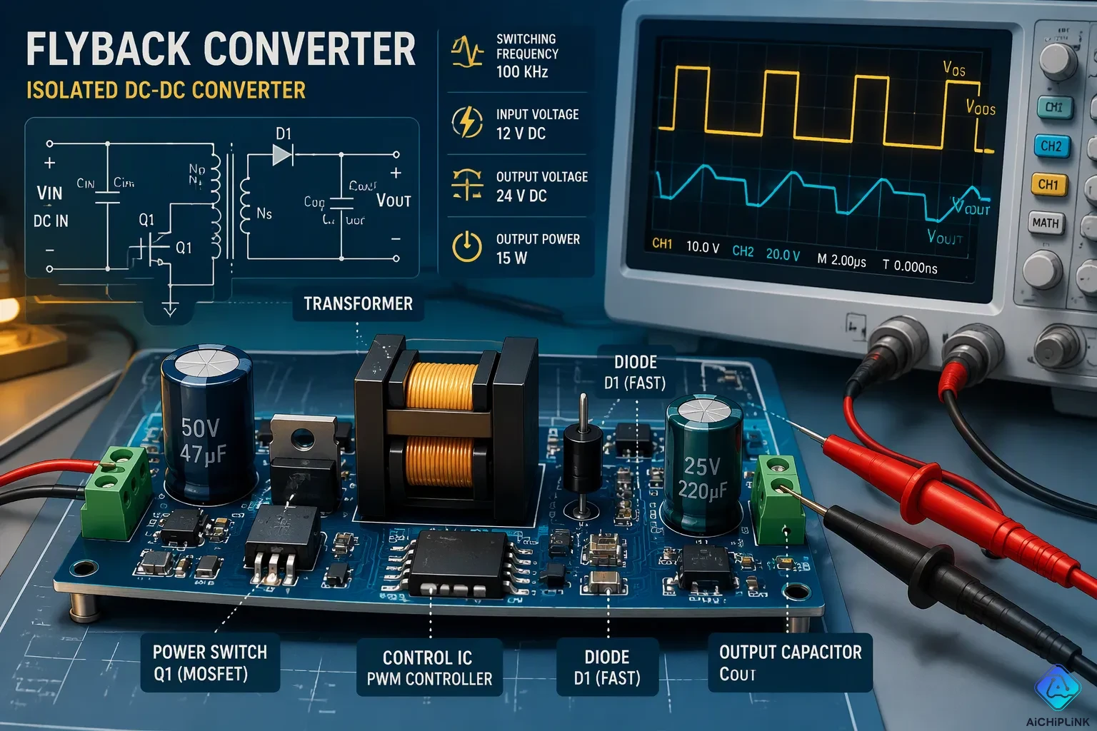
A flyback converter circuit pairs a power supply IC with a small set of key parts. These include the primary switch, transformer, output rectifier, input and output capacitors, VH pin resistor, AC start/stop divider, noise reduction capacitors, and feedback network. Each part shapes the voltage waveform and how the whole circuit behaves.
AC-DC adapters are a top application segment, holding a 34% market share with 5.9% growth. Because they are so popular, flyback DC/DC converters are a common starting point for engineers.
| Segment | Position | Market Share | Growth Rate |
|---|---|---|---|
| AC-DC Adapters | Leading | 34% | 5.9% |
You will learn how each of these components works and how to choose its parameters, with practical guidelines and typical values. Your goal: pick values that keep voltage steady and ensure operation, efficiency, and reliability.
Key Takeaways
-
The transformer turns ratio sets the voltage stress on the switch and affects efficiency. Choose it carefully to balance stress and duty cycle.
-
The VH pin resistor gives the startup current and sets the start and stop voltages. Choose a value between 5 kΩ and 60 kΩ so the circuit starts reliably.
-
Noise reduction capacitors, such as snubbers and bypass capacitors, help control voltage spikes and ripple. Put them close to the switch and rectifier so they work their best.
-
The feedback network uses an optocoupler and TL431 to keep the output voltage steady. Adjust the compensation components to make sure the circuit runs stably.
-
Follow a step-by-step design flow: define specifications, choose turns ratio, calculate currents, select components, and verify on the bench. This approach makes design repeatable and reliable.
Power Stage of the Flyback Converter Circuit
The power stage of a flyback converter circuit has five parts: the primary switch (usually a MOSFET), the transformer (a mutually coupled inductor), the output rectifier, the input capacitor, and the output capacitor. The power supply IC drives the switch at a steady switching frequency fs. Energy is stored in the transformer during the on-time and moves to the secondary during the off-time. In the steady state, the output voltage follows Vout = Vin x (Ns/Np), where Np and Ns are the primary and secondary winding counts. Transformer design strongly affects efficiency and EMI performance, so treat it as the heart of the power stage.
Transformer Turns Ratio and Inductance
The turns ratio sets the reflected voltage. The relation is Vor / (Vout + Vd) = Np/Ns, where Vd is the rectifier forward drop. A lower reflected voltage cuts switch voltage stress, yet it forces a longer duty cycle. A higher reflected voltage calls for a higher peak inverse voltage rating on the diode. You also trade primary ripple current against secondary ripple current. The switch stress follows Vswitch = Vin + Vout/N. With 48V input and 12V output at N = 0.25, the stress is 48 + 12/0.25 = 96V, so you need at least a 150V MOSFET.
Primary inductance and its tolerance matter just as much. Gapped ferrite keeps inductance within 10% across the extended temperature range. Ungapped ferrite swings by roughly 200%, which makes the design unpredictable.
| Core Type | Inductance at Room Temp | Inductance at –40°C | Inductance at 120°C | Tolerance Over Extended Temp Range |
|---|---|---|---|---|
| Gapped ferrite | 300 µH | 285 µH | 311 µH | Within 10% |
| Ungapped ferrite | 300 µH | 170 µH | 570 µH | ~200% variation |
Selecting Critical Components: Switch and Rectifier
When you select critical components, start with the MOSFET ratings. Check the maximum drain-source voltage, the peak current, the conduction loss from on-resistance, and the package power dissipation. Compute Vds(max) = Vin(max) + VOR + Vspike, where Vin(max) is the peak of the highest AC input, VOR is the reflected output voltage, and Vspike is the snubber-clamped spike. A common rule of thumb picks Ids at about twice the primary peak current. A 2.32A peak therefore points to roughly 4.64A, which suits an 800V/5A part such as the R8005ANX (Ron = 1.6Ω, TO-220F). Check Vds, Ids, and heat on the bench afterward.
The output rectifier deserves equal care. Its parasitic reverse-recovery charge and nonlinear capacitance add switching loss and cause ringing during commutation. Cutting that charge lowers loss and boosts efficiency.
VH Pin Resistor and Startup Current
Role of the VH Pin Resistor
At power-up, the power supply IC has no energy of its own. The VH pin resistor bridges this gap. It connects the rectified high voltage rail to the VH pin and feeds a small current into the controller. This current charges the supply rail and wakes the internal startup circuit. Once the auxiliary winding produces enough voltage, the controller draws its own power and the resistor steps back.
This handover matters for efficiency. A resistor that feeds too much current wastes power during normal operation. A resistor that feeds too little current leaves the startup circuit stalled. The VH pin resistor also acts as a safety element. It limits current if the VH pin shorts to ground.
Calculating Resistor Value and Power Rating
Size the resistor from the voltage at the VH pin and the current the controller needs. The pin sees the AC line multiplied by √2, so the voltage spans the full 85 to 264 VAC range. The datasheet lists a startup current of up to 5 mA. Follow these steps:
-
Multiply the AC input voltage by √2 to find the peak voltage at the VH pin.
-
Divide that peak voltage by the required startup current to get the upper resistance limit.
-
Check the lower limit against the current-limiting requirement for a shorted VH pin.
-
Confirm the result lands within the 5 kΩ to 60 kΩ range.
For a typical design, a 10 kΩ resistor fits this window. The part must also survive the full input voltage and the power dissipation equal to resistance times current squared. Choose a resistor with a generous power margin, and verify the startup circuit behavior on the bench across the full line range.
Setting AC Start and Stop Voltages
How the Start/Stop Divider Works
The VH pin does two jobs. It supplies startup current, and it reads the rectified line level. A resistor divider runs from the high-voltage rail to the VH/AC sense pin. This divider sets the two thresholds that decide when the power supply IC turns on and when it turns off. You choose the top and bottom resistors so the divided voltage crosses the internal reference at the line level you want.
The start threshold is the lowest input voltage where the controller begins switching. The stop threshold is the level where it stops. A wide gap between the two keeps the supply from chattering when the line sags. This gap is called hysteresis, and many controllers build it in internally. Some parts let you add external hysteresis with a feedback resistor or a small capacitor at the sense pin. Check the datasheet before you add parts.
Choosing Divider Resistor Values
Start with the internal reference and the start level you want. The divider ratio equals the reference divided by the peak of your chosen start voltage. Keep the total resistance high enough to limit bleed current, but low enough that leakage and noise do not shift the threshold. The 5 kΩ to 60 kΩ window used for the VH resistor gives you a practical starting range.
Check the stop level after you fix the ratio. Make sure the resulting start/stop voltages fall inside your AC line range. Also make sure the startup circuit still delivers enough current at the low line. Build the divider on a breadboard and sweep the line slowly. Watch for a clean single transition at each threshold. The turns ratio, duty cycle, and switching frequency stay fixed here, but a wrong divider can still stall the supply before it ever reaches regulation.
Noise Reduction Capacitors
Snubber and Bypass Capacitor Roles
A snubber capacitor sits right across the primary switch. It gives the drain current an easy path during turn-off, and that path slows the voltage change. The capacitor also catches energy stored in stray and leakage inductance before it can form a spike. In an RCD clamp, the capacitor clamps the drain spike caused by leakage inductance resonating with the MOSFET output capacitance. The clamp voltage usually sits at about 2 to 2.5 times the reflected output voltage. A series resistor limits the discharge peak current at turn-on and damps the LC ringing.
| Role | Mechanism | Effect on Spikes |
|---|---|---|
| Limits dV/dt | Low-impedance path slows the turn-off transition | Reduces the steepness of the excursion |
| Absorbs stray-inductance energy | Captures leakage energy before it spikes | Prevents a high-voltage spike |
| Suppresses ringing | Alternative current path damps LC oscillation | Keeps drain-source voltage near the bus level |
Bypass capacitors do a different job. The input capacitor keeps the rectified rail steady and supplies the current pulses the switch needs. The output capacitor smooths the secondary current and sets the output voltage ripple. Both parts also send high-frequency noise away from sensitive nodes.
Typical Capacitor Values and Placement
Place the snubber capacitor close to the switch, with short leads, so the loop inductance stays low. Keep the input capacitor near the transformer primary and the output capacitor near the rectifier. Short, tight loops cut radiated noise. Choose the output capacitor for its ripple current rating, not just its capacitance. The output ripple depends on capacitance, ESR, and the duty cycle. A larger output capacitor lowers voltage ripple, but it also raises inrush stress. Balance the two.
The switching frequency and turns ratio set the ripple current the capacitors must handle. Check voltage ripple on the bench across the full line range. These components work as a system, and input and output capacitors together decide how quiet the supply runs.
Feedback Network in Isolated Flyback Converter Circuits
Optocoupler and TL431 Configuration
An isolated flyback converter circuit needs a feedback path that crosses the isolation barrier. The optocoupler and the TL431 shunt regulator make up that path. The TL431 reads the output voltage through a divider, and it drives the optocoupler LED. The optocoupler transistor then pulls on the power supply IC feedback pin. This setup keeps the secondary side electrically separate from the primary side.
You set the output voltage with two output voltage setting resistors at the TL431 reference pin. The divider ratio fixes the regulation point. Pick resistor values that keep the divider current well above the TL431 minimum operating current. A small bypass capacitor across the upper resistor filters switching noise before it reaches the reference pin.
Compensation Component Selection
Loop stability depends on the compensation components around the TL431. A resistor and capacitor network from the TL431 cathode to its reference pin shapes the error amplifier response. The capacitor sets the low-frequency gain roll-off. The resistor sets the mid-band gain. A second capacitor often sits in parallel to roll off high-frequency gain and suppress noise.
Start with a target crossover frequency well below the switching frequency, usually one-tenth or less. Then size the compensation capacitor so the loop gain crosses zero with enough phase margin. Check the result on the bench with a loop gain measurement. Watch the transient response at the output capacitor terminals. A slow recovery points to insufficient bandwidth. Ringing points to poor phase margin. Adjust the resistor and capacitor values in small steps until the response settles cleanly. The turns ratio and output voltage ripple also shift the plant gain, so verify stability at both low line and high line.
Flyback Converter Design and Calculation
Step-by-Step Parameter Flow
You can design a flyback converter with a power supply IC by following a set order. Begin with the input voltage range, output voltage, maximum load current, and switching frequency. These four numbers guide every choice you make later. Next, choose the turns ratio and keep the duty cycle under about 60% to limit peak currents. Then figure out the ripple and peak currents using a ripple factor between 0.3 and 0.6. Make sure the transformer saturation current is higher than the peak current you found.
Now pick the capacitors. Choose an input capacitor with low impedance at the switching frequency and a good ripple current rating. Size the output capacitor for voltage ripple and load-step needs, and put parts in parallel when the RMS current runs high. Add common-mode chokes and Y-capacitors to cut down EMI. Finish by checking output ripple and load-step response on an oscilloscope, then adjust the layout or filters if you miss your targets. This flow keeps flyback converter design and calculation neat and repeatable.
Design Example for PWM Flyback Converter
Here is a design example for PWM flyback converter work with real numbers. Suppose you have a 48V to 12V, 2.5A, 30W DCM stage at 100kHz with 85% efficiency and a Schottky forward drop of 0.5V. The duty cycle is (12 + 0.5)/(48 + 12 + 0.5), about 0.207. The peak primary current is (2 × 30W)/(0.85 × 48V × 0.207), about 7.09A. Primary inductance is (48V × 0.207)/(7.09A × 100kHz), about 14.0µH. A turns ratio of 0.25 works, for example 35 primary turns and 9 secondary turns on an ETD29 core with a 2.5mm air gap.
Switch stress is 48 + 12/0.25 = 96V, so a 150V FET is the lowest rating you can use. Primary RMS current is about 1.86A, which fits 20AWG wire or Litz. Secondary RMS current is about 3.54A, which fits 18AWG. Keep output capacitor ESR under 50mΩ for low ripple. When you pick critical components on the secondary side, use about 70% derating: 87V ÷ 0.7 = 124V, so choose a 200V fast diode such as the RF1001T2D. Run it at 50% or less of rated current, and estimate loss as 1V × 3A = 3W.
A typical AC-input spec sheet lists 85 to 264 VAC input, 12VDC ±5% at 3A, 200mVp-p output voltage ripple, 3kVAC isolation, and 80% or higher efficiency. Transformer design and the output capacitor choice drive most of the remaining performance. Flyback DC/DC converters succeed or fail on these parameters, so check each one on the bench.
Every part in a flyback converter circuit has a job to do. The turns ratio sets the switch stress. The divider resistors fix the start and stop points. The output capacitor controls voltage ripple, and the compensation network keeps the output voltage steady. When you get these values right, you gain efficiency, stability, and reliability.
Think of flyback converter design and calculation as one connected task. No single component stands alone here. A new turns ratio changes the stress and the ripple current. Check each choice against datasheet limits. Then confirm the result on the bench. What you measure on the bench beats a clean spreadsheet every time.

Written by Jack Elliott from AIChipLink.
AIChipLink, one of the fastest-growing global independent electronic components distributors in the world, offers millions of products from thousands of manufacturers, and many of our in-stock parts is available to ship same day.
We mainly source and distribute integrated circuit (IC) products of brands such as Broadcom, Microchip, Texas Instruments, Infineon, NXP, Analog Devices, Qualcomm, Intel, etc., which are widely used in communication & network, telecom, industrial control, new energy and automotive electronics.
Empowered by AI, Linked to the Future. Get started on AIChipLink and submit your RFQ online today!
Frequently Asked Questions
What sets the output voltage in a flyback converter circuit?
The transformer turns ratio and the feedback divider at the TL431 set the output voltage. The controller adjusts duty cycle to hold regulation. Check the output voltage at both low line and high line, because plant gain shifts across the input range.
How do I pick the VH pin resistor value?
Aim for the 5 kΩ to 60 kΩ window listed in the datasheet. A 10 kΩ part is a common choice. Confirm the startup current reaches the controller at the lowest line voltage, and give the resistor power margin for the full input voltage.
Which components limit switch stress?
The turns ratio and the RCD clamp do most of this work. With 48V input and 12V output at a 0.25 ratio, stress reaches 96V, so a 150V MOSFET is the minimum. Set the clamp near 2 to 2.5 times the reflected voltage.
Why does flyback layout matter for noise?
A tight flyback layout keeps the snubber loop and the input capacitor loop short. Short loops cut radiated noise and drain spikes. Place the output capacitor close to the rectifier. A poor flyback layout raises EMI, and no capacitor value can fully fix it.
How do I check loop stability?
Target a crossover frequency at one-tenth of the switching frequency or lower. Measure loop gain on the bench. A slow transient recovery means low bandwidth. Ringing means poor phase margin. Adjust the TL431 compensation resistor and capacitor in small steps.