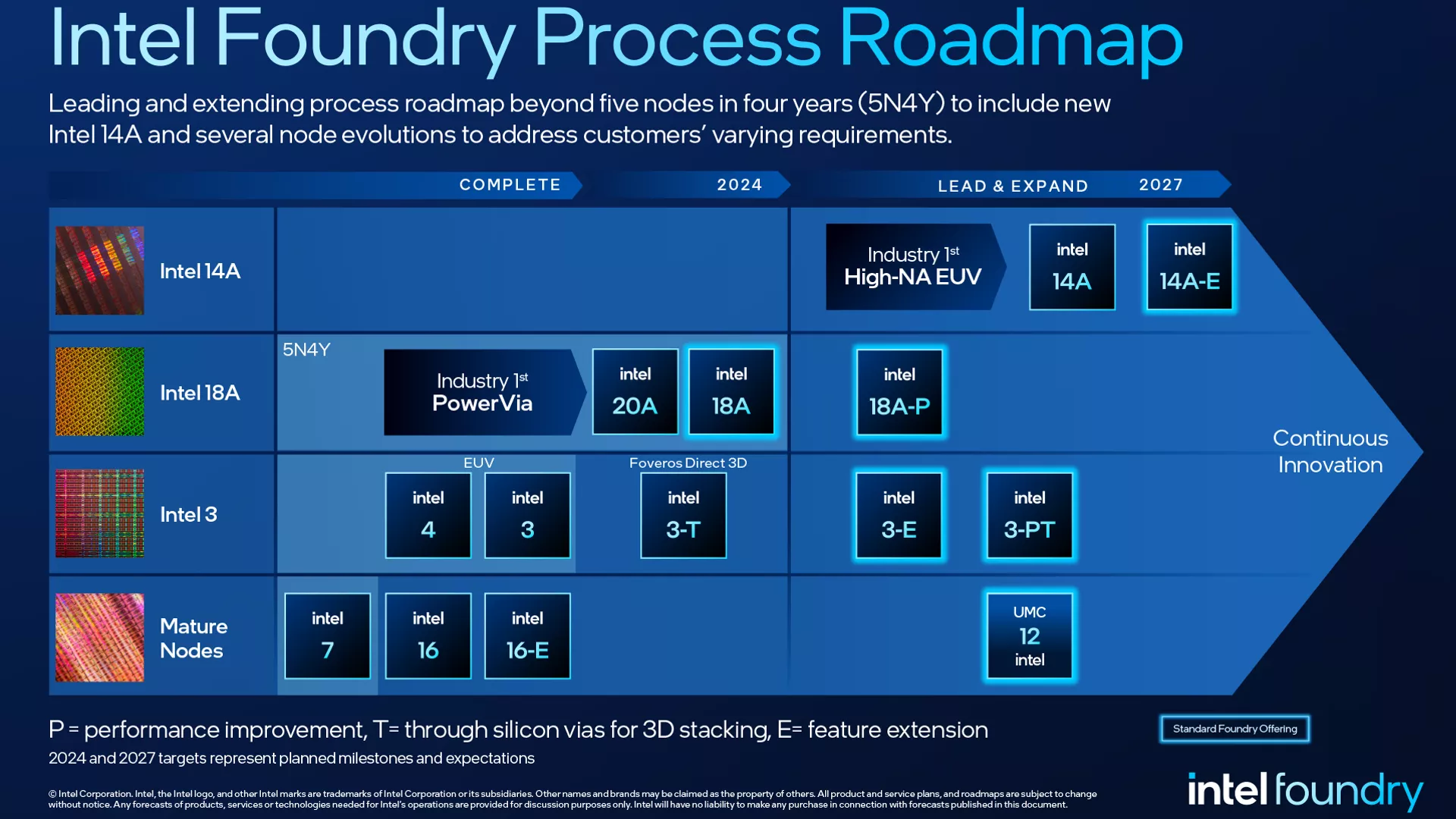
As Intel races to regain semiconductor leadership, its roadmap through 2025 stands as both a bold vision and a high-stakes gamble. Under CEO Pat Gelsinger’s leadership, Intel is transitioning through five process nodes in just four years—a blistering pace that repositions the company in a rapidly evolving industry. From Intel 7 to Intel 18A, each step brings dramatic changes in lithography, transistor architecture, power delivery, and manufacturing strategy.
In this in-depth blog, we’ll dissect Intel’s entire roadmap, the technological innovations behind each node, and how these advancements influence performance, efficiency, and Intel's competitiveness against TSMC, Samsung, and AMD.
The Context Behind Intel's Roadmap
In Intel's roadmap, the company has made significant progress in its transition to new fabrication processes. Intel 7 and Intel 4 have been completed, with Intel 3, 20A, and 18A coming in the next few years. Intel 7 is the company's 10nm process, and Intel 4 is its 7nm process. The names can be misleading, but nanometer measurements in chips are now mostly marketing terms.
Intel was once the undisputed leader in semiconductor manufacturing, but a series of delays in transitioning from 14nm to 10nm and the subsequent struggle to catch up with 7nm eroded confidence. Competitors like AMD (using TSMC's advanced nodes) surged ahead in performance and efficiency, while Intel remained stuck with legacy technology.
To reverse this trajectory, Intel introduced its IDM 2.0 strategy, emphasizing three pillars:
1. Internal manufacturing: Continue building in-house chips.
2. External manufacturing: Outsource some components to TSMC and others.
3. Intel Foundry Services (IFS): Provide foundry capacity to third parties, like Qualcomm and MediaTek.
The cornerstone of this strategy is Intel's promise of “5 nodes in 4 years,” aggressively transitioning from Intel 7 to 18A by 2025.
Overview of Intel’s Process Nodes
Intel’s rebranding of its process nodes reflects a shift in marketing and technical alignment. Previously, Intel’s 10nm process was numerically behind TSMC’s 7nm, even though the performance was comparable. To address confusion, Intel began naming nodes based on industry-relative performance rather than gate pitch or traditional metrics.
| Node | Release Timeline | Node Type | Major Technologies |
|---|---|---|---|
| Intel 7 | 2021–2022 | FinFET | Hybrid architecture, SuperFin enhancements |
| Intel 4 | 2023–2024 | FinFET + EUV | Full EUV adoption, 20% perf/watt boost |
| Intel 3 | 2024 | FinFET + EUV+ | More EUV layers, optimized power and density |
| Intel 20A | 2024–2025 | RibbonFET | GAA transistors, backside power delivery |
| Intel 18A | 2025 | RibbonFET+ | Enhanced GAA, High-NA EUV, foundry-ready |
Each of these nodes is a stepping stone toward Intel's ambitious comeback.
Intel 7: The Alder Lake and Raptor Lake Era
Intel 7 is the last process from Intel to use deep ultraviolet lithography, or DUV. Intel 7 was used to produce Alder Lake, Raptor Lake, and the recently announced Raptor Lake Refresh that arrived alongside Meteor Lake. Meteor Lake, however, is produced on Intel 4.
• Launch Timeline: Q4 2021 – 2023
• Manufacturing Platform: 10nm Enhanced SuperFin (renamed Intel 7)
• Transistor Technology: FinFET
• Performance Gain Over Previous Node: ~10–15%
Intel 7 was Intel’s first serious step back into competitiveness. It’s essentially an enhanced version of 10nm SuperFin, with better drive currents and improved transistors. Though it lacked EUV lithography, Intel 7 enabled the debut of the hybrid architecture that would define modern Intel CPUs.
Key Innovations:
• Hybrid CPU cores (P-cores + E-cores) — Performance and Efficiency cores in a single package.
• Intel Thread Director — OS-level optimizations for hybrid workloads.
• DDR5 & PCIe 5.0 Support — Modern I/O interfaces became standard.
Products:
• Alder Lake (12th Gen Core) — Major success, especially in gaming desktops.
• Raptor Lake (13th Gen Core) — Incremental improvements with more E-cores, cache, and higher clocks.
Intel 7 brought Intel back to performance parity, setting the stage for architectural and manufacturing overhauls.
Intel 4: The Era of EUV and Meteor Lake
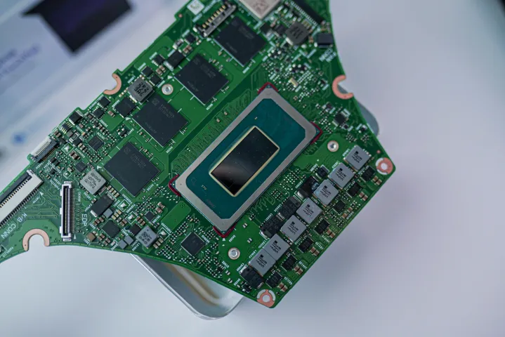
Intel 4 is the near future unless you're a laptop user, in which case, it's the present. Meteor Lake is fabricated on Intel 4... mostly. The computer Tile of Meteor Lake's new CPUs are fabricated on Intel 4, but the graphics Tile is fabricated on TSMC N3. These two tiles (along with the SoC Tile and the I/O Tile) are integrated using Intel's Foveros 3D packaging tech. This process is typically referred to as disaggregation and the AMD equivalent is called a chiplet.
• Expected Volume Production: Late 2023 – Early 2024
• Technology Used: Full EUV adoption
• Performance Improvement: ~20% per watt over Intel 7
• Transistor Type: FinFET with smaller library and tighter pitches
Intel 4 marks Intel's first full adoption of extreme ultraviolet (EUV) lithography, drastically reducing the number of multi-patterning steps and enabling higher yield and lower cost at advanced geometries.
Meteor Lake — A Major Shift in Design
Meteor Lake introduces Intel’s most modular CPU yet, consisting of multiple tiles (chiplets) built on different nodes and stitched together with Foveros 3D stacking.
Tiles:
• Compute Tile (Intel 4) — Houses P-cores and E-cores
• Graphics Tile (TSMC N5) — Arc-based GPU
• SoC & I/O Tiles — Handle memory, power, and security
Advantages:
• Higher power efficiency for mobile systems
• Dynamic power management per tile
• Greater flexibility in die combinations
Meteor Lake also introduces AI and media acceleration, targeting premium ultrabooks and thin laptops.
Intel 3: Incremental Refinement for Data Centers
Intel 3 is a follow-on from Intel 4 but brings with it a roughly 18% performance per watt gain over Intel 4. It has a denser high-performance library but is only aimed at data center usage so far with Sierra Forest and Granite Rapids. Intel's Sierra Forest Xeon 6 processors use this node, and so do Intel's Granite Rapids processors, too.
• Expected Production: 2024
• Lithography: Enhanced EUV with more layers
• Performance Gain: Higher drive currents, improved density over Intel 4
• Use Case: Xeon server CPUs
Intel 3 refines Intel 4’s design, using:
• More EUV layers to reduce pattern complexity
• New cell libraries for higher density
• Better metallization and power efficiency
Intel 3 is optimized for server-class workloads and will power:
• Sierra Forest — E-core-only Xeon CPU
• Granite Rapids — P-core Xeon for high-performance computing
Intel claims Intel 3 is on track with yields improving as of early 2024.
Intel 20A: RibbonFET and PowerVia Redefine the Silicon Stack
Intel 20A is a semiconductor process node named for its approximate transistor gate length of 20 angstroms (2 nanometers). It was planned as a major leap in Intel’s manufacturing roadmap, marking the company’s entry into the Angstrom Era—where nodes are measured in angstroms rather than nanometers.
• Expected Ramp: Late 2024 – Early 2025
• Transistor Technology: RibbonFET (GAA)
• Power Delivery: PowerVia (backside power)
• Major Leap: From FinFET to gate-all-around
Intel 20A is where the Ångström Era begins. The name "20A" refers to 20 Ångström, equivalent to 2nm — though not strictly defined by physical gate length.
RibbonFET: Intel’s GAA Breakthrough
• Intel’s first new transistor architecture since FinFET (2011)
• Enables multiple stacked nanosheets (“ribbons”) per transistor
• Provides better electrostatic control and performance at lower voltages
PowerVia: Industry-first Backside Power Delivery
• Moves power rails to the back of the wafer
• Reduces voltage droop and resistance
• Frees frontside for signal routing
This combination improves frequency, energy efficiency, and die area — unlocking major performance scaling.
Intel 18A: Foundry-Ready Node for the Future
Intel 18A stands for 18 angstroms, or 1.8 nanometers, and represents a crucial step in Intel’s roadmap toward regaining semiconductor process leadership. It's the successor to Intel 20A and retains its key innovations—RibbonFET and PowerVia—with further optimizations.
Expected Production: 2025
Enhancements:
• Refined RibbonFET
• Optimized PowerVia
• High-NA EUV (potential)
Intel 18A is a maturity node — not just for Intel's own CPUs, but also for Intel Foundry Services (IFS). With Qualcomm already committed as a customer, 18A is being developed with foundry requirements from day one.
Key improvements:
• Greater drive current per transistor
• Shorter gate pitch
• Better performance per watt vs 20A
• Use of high-numerical-aperture (High-NA) EUV lithography
Intel is positioning 18A as the node where it will reclaim leadership and open its fabs to world-class customers like Qualcomm, MediaTek, and Amazon.
Comparison: Intel Process Nodes (2021–2025)
Between 2021 and 2025, Intel significantly revamped its process node roadmap to regain semiconductor leadership. Starting with Intel 7 (formerly 10nm Enhanced SuperFin), it advanced to Intel 4 and Intel 3, introducing EUV lithography and enhanced FinFET performance. In 2024, Intel 20A brought major breakthroughs with RibbonFET (Intel’s gate-all-around transistor) and PowerVia (backside power delivery). By 2025, Intel 18A refines these innovations and is designed for high-volume manufacturing, positioning Intel to compete directly with leading foundries like TSMC and Samsung.
| Feature | Intel 7 | Intel 4 | Intel 3 | Intel 20A | Intel 18A |
|---|---|---|---|---|---|
| Launch Year | 2021–2022 | 2023–2024 | 2024 | 2024–2025 | 2025 |
| Transistor Type | FinFET | FinFET | FinFET (refined) | RibbonFET (GAA) | RibbonFET+ |
| EUV Support | No | Full EUV | More EUV layers | Full EUV | High-NA EUV (planned) |
| Power Delivery | Frontside | Frontside | Frontside | PowerVia (Backside) | Enhanced PowerVia |
| Performance Boost | ~10–15% | ~20% | Incremental | Major leap | Industry-leading |
| Key Product | Alder, Raptor Lake | Meteor Lake | Sierra/Granite Rapids | Arrow Lake | Lunar Lake, Foundry SoCs |
Intel’s CPU Architectural Roadmap
Intel's CPU Architectural Roadmap lays out the company's planned evolution of microprocessor architectures over time, typically spanning several generations. As of 2025, Intel has publicly shared details of its roadmap through 2025 and beyond, including the evolution from Intel 7 through to Intel 18A, aligning with its aggressive "five nodes in four years" strategy to reclaim process leadership.
| Architecture | Node | Key Product | Notable Features |
|---|---|---|---|
| Alder Lake | Intel 7 | 12th Gen Core | Hybrid x86, DDR5/PCIe 5.0 |
| Raptor Lake | Intel 7 | 13th Gen Core | More E-cores, higher boost |
| Meteor Lake | Intel 4 | 14th Gen (Mobile) | Chiplet design, AI engine |
| Arrow Lake | Intel 20A | 15th Gen (Desktop/Mobile) | RibbonFET + PowerVia |
| Lunar Lake | Intel 18A | 16th Gen (Ultraportable) | Ultra-low power, AI/graphics improvements |
Frequently Asked Questions (FAQ)
Q1: What does Intel 7 mean?
Intel 7 is the rebranded name for Intel’s 10nm Enhanced SuperFin process. It offers ~10–15% performance per watt gains over 10nm and was used for Alder and Raptor Lake CPUs.
Q2: Why is EUV so important in Intel 4?
EUV simplifies patterning at smaller geometries, reduces cost, and improves yield. Intel 4 is the first Intel node to fully embrace EUV lithography.
Q3: What makes RibbonFET different from FinFET?
RibbonFET is a gate-all-around (GAA) transistor where the gate fully surrounds the channel. It offers superior electrostatic control, better scaling, and energy efficiency at nanoscale dimensions.
Q4: What is PowerVia, and who else uses it?
PowerVia is Intel's proprietary backside power delivery method. While Samsung and TSMC are exploring similar ideas, Intel is the first to implement it at scale.
Q5: Will Intel succeed in delivering 5 nodes in 4 years?
As of 2025, Intel appears on track, with Meteor Lake (Intel 4) shipping and Intel 3 and 20A in late-stage development. Industry observers remain cautiously optimistic.
Q6: What’s the role of Intel Foundry Services?
IFS is Intel’s bid to become a top-tier global foundry, rivaling TSMC. Customers like Qualcomm and MediaTek plan to use Intel nodes, starting with Intel 18A.

Conclusion
Whether Intel will retain its progressive additions going forward remains to be seen, but it bodes well that the only change the company has had to make was to make its most advanced node launch even sooner than anticipated. While it's not clear whether Intel will be a formidable competitor to TSMC and Samsung still when it comes to its more advanced processes (especially when it reaches RibbonFET), we're certainly hopeful. Meteor Lake has been a good start, Lunar Lake has been even better, but who knows what lies in the future after Arrow Lake.
Intel’s roadmap from Intel 7 through Intel 18A is more than just a technological journey — it’s a resurrection arc. With EUV, RibbonFET, PowerVia, and aggressive node development, Intel aims not only to regain parity with competitors like TSMC and Samsung but to leap ahead.
If successful, Intel will not only dominate the client and server CPU markets but become a powerhouse foundry for global tech giants. The road to 2025 is paved with innovation, risk, and opportunity — and Intel is betting big on all three.
Written by Jack Zhang from AIChipLink.
AIChipLink, one of the fastest-growing global independent electronic component distributors in the world, offers millions of products from thousands of manufacturers, and many of our in-stock parts is available to ship same day.
We mainly source and distribute integrated circuit (IC) products of brands such as Broadcom, Microchip, Texas Instruments, Infineon, NXP, Analog Devices, Qualcomm, Intel, etc., which are widely used in communication & network, telecom, industrial control, new energy and automotive electronics.
Empowered by AI, Linked to the Future. Get started on AIChipLink.com and submit your RFQ online today!