
Integrated circuit design forms the foundation of modern electronics. Devices today rely on chips that contain over a billion transistors, with each chip following more than 500 manufacturing rules.
| Numerical Data Point | Value/Description |
|---|---|
| Number of transistors in a desktop chip (2015) | Over 1 billion |
| Number of manufacturing rules (2015) | More than 500 |
Advances in integrated circuit technology have achieved over 40% higher operating frequency in some devices. However, designers face challenges such as balancing power, performance, and area, while also managing growing complexity and unpredictable device behavior.
Key Takeaways
-
Integrated circuit design tries to balance power, speed, and size.
-
This helps make chips that work well in today’s devices.
-
Power management methods save battery and keep chips cool.
-
Examples are changing voltage and turning off parts not used.
-
Good signal and heat control help circuits work right and last longer.
-
These are important when chips run fast and get hot.
-
Making chips smaller and stacking them adds more features.
-
This lets us have tiny but strong electronics.
-
Engineers use different ways to design chips.
-
Some ways are custom, others can be changed after making.
-
These choices help make chips faster, cheaper, or more flexible.
Core Design Principles in Integrated Circuit Design
Power Management Strategies
Power management stands as a central concern in integrated circuit design. Engineers focus on reducing energy consumption while maintaining high performance. The demand for energy-efficient devices, electric vehicles, and advanced consumer electronics drives innovation in this area. Market data shows that the power management IC market reached $43.82 billion in 2024, with projections of $70.96 billion by 2033. This growth reflects the ongoing improvements in power management strategies and the adoption of new technologies.
| Year | Market Size (USD Billion) | CAGR (%) | Remarks |
|---|---|---|---|
| 2024 | 43.82 | 5.5 | High integration and efficiency in power management ICs. |
| 2025 | 46.24 (forecast) | 5.5 | Growth driven by smartphones, automotive, and 5G rollout. |
| 2033 | 70.96 (projected) | 5.5 | Linked to technological advancements and battery demand. |
Designers use techniques such as dynamic voltage scaling, clock gating, and power gating to optimize energy use. These methods help extend battery life and reduce heat generation. The use of process design kits (PDKs) from foundries supports the creation of efficient circuits by providing accurate manufacturing data and standard cell libraries. Customer-owned technology (COT) models allow companies to tailor power, area, and cost trade-offs for specific applications. These strategies ensure that integrated circuits meet the needs of modern devices without sacrificing reliability or performance.
Tip: Effective power management not only improves device longevity but also lowers manufacturing costs and supports environmental sustainability.
Signal Integrity Considerations
Signal integrity plays a vital role in ensuring that integrated circuits function correctly at high speeds. As circuits become smaller and faster, issues such as crosstalk, noise, and voltage drops can disrupt signal transmission. Research from leading universities validates the use of advanced modeling and simulation tools to address these challenges. Engineers employ incremental static timing analyzers, cross-coupling RC extractors, and waveform calculators to predict and mitigate noise and delay.
-
Validation of crosstalk modeling enables accurate prediction of switching effects.
-
Early-stage crosstalk avoidance during placement and routing reduces costly post-layout fixes.
-
Practical strategies include adding spacing, shielding, and routing constraints to minimize interference.
-
IR drop analysis tools detect voltage drop issues early, allowing for timely power network adjustments.
-
Electromigration analysis ensures that interconnects can handle current flow without failure.
-
Inductance mitigation techniques, such as shielding clock signals and inserting ground returns, further enhance signal integrity.
These empirical approaches, now integrated into electronic design automation (EDA) tools, have been verified through simulation and prototype testing. By focusing on signal integrity, designers can achieve higher performance and reliability in integrated circuits.
Miniaturization and Density
Miniaturization and increased component density define the progress of integrated circuit design. The industry has moved from small-scale integration (SSI) to very-large-scale integration (VLSI), now packing billions of transistors onto a single chip. Advanced fabrication processes, such as 5nm and 3nm nodes, enable higher transistor density and improved performance. Three-dimensional stacking techniques, like through-silicon vias (TSVs), allow engineers to build vertically, surpassing the limits of traditional planar layouts.
| Benchmark Aspect | Evidence / Description |
|---|---|
| Transistor Integration Scale | Progression from SSI to VLSI with millions to billions of transistors on a single chip. |
| Nanometer Technologies | Adoption of 5nm and 3nm nodes for higher density and performance. |
| 3D Stacking Techniques | Use of TSVs to vertically stack silicon dies, increasing density. |
| Miniaturization Benefits | Smaller device size, higher speed, improved power efficiency, and cost reduction. |
| System-on-Chip (SoC) Evolution | Integration of CPU, memory, and I/O on a single chip. |
| MEMS Technology | Micro-electro-mechanical systems compact mechanical functions, enhancing miniaturization. |
| Thermal Management | Advanced cooling solutions support high-density designs. |
Miniaturization allows for smaller, lighter devices with greater functionality. For example, satellites now use compact, high-quality components that reduce launch costs and increase capabilities. The use of advanced printed circuit board (PCB) materials and micro-electro-mechanical systems (MEMS) further boosts component density. Designers must also address thermal management, using materials and cooling techniques to maintain performance and prevent damage in densely packed circuits.
Note: The evolution of system-on-chip (SoC) technology represents a major leap in complexity and density, integrating entire systems onto a single chip.
Durability and Reliability Factors
Durability and reliability stand as essential goals in integrated circuit design. Engineers must ensure that each integrated circuit can withstand years of operation without failure. They focus on several factors that influence long-term performance and reliability.
-
Material Selection: Designers choose materials that resist wear, corrosion, and electrical breakdown. Silicon remains the most common material, but advanced circuits may use silicon carbide or gallium nitride for higher durability.
-
Environmental Stress Testing: Engineers expose circuits to temperature extremes, humidity, and vibration. These tests simulate real-world conditions and help identify weaknesses before mass production.
-
Electromigration Prevention: High current densities can cause atoms in metal interconnects to move, leading to circuit failure. Designers use wider traces and robust materials to prevent this problem.
-
Redundancy and Error Correction: Some designs include redundant circuits or error-correcting codes. These features allow the integrated circuit to continue working even if part of it fails.
-
Aging and Degradation Analysis: Engineers study how circuits age over time. They use accelerated life testing to predict failures and improve future designs.
Tip: Reliable integrated circuits reduce maintenance costs and increase consumer trust in electronic products.
Durability and reliability factors directly affect the integrity of the device. A robust design ensures that the integrated circuit maintains high performance and reliability throughout its lifespan.
Thermal Management in Integrated Circuits
Thermal management plays a critical role in integrated circuit design. As circuits become smaller and more powerful, they generate more heat in a confined space. Excessive heat can degrade performance, shorten lifespan, and cause sudden failures.
Engineers use several strategies to manage heat:
-
Heat Sinks and Spreaders: These components draw heat away from the chip and disperse it into the surrounding environment.
-
Thermal Interface Materials: Special materials fill gaps between the chip and heat sink, improving heat transfer.
-
On-Chip Cooling: Some designs include microchannels or embedded cooling systems to remove heat directly from the chip.
-
Dynamic Power Management: By adjusting power usage based on workload, circuits can reduce heat generation during low-demand periods.
Numerical analysis confirms the efficiency of these thermal management techniques. Metrics such as θJA (junction-to-ambient), θJC (junction-to-case), and θCA (case-to-ambient) measure how well heat moves away from the semiconductor junction. Lower thermal resistance values indicate better heat dissipation. Engineers use steady-state and transient thermal analyses to calculate junction temperatures and temperature gradients. These calculations help predict device reliability and prevent overheating.
Advanced simulation tools, such as the Cadence Celsius Thermal Solver, combine finite element analysis (FEA) and computational fluid dynamics (CFD). These tools simulate both current and heat flow, allowing engineers to detect and fix thermal issues early in the design process. They provide detailed temperature profiles and identify hotspots in complex 3D integrated circuits.
| Numerical Method | Purpose | Key Parameters | Outcome |
|---|---|---|---|
| Finite Element Analysis (FEA) | Predict temperature profiles in 3D ICs | TSV diameter, pitch, SiO2 thickness | Accurate thermal conductivity estimation; improved efficiency |
| Computational Fluid Dynamics (CFD) | Analyze heat dissipation and fluid flow | Natural convection conditions | Evaluates heat dissipation in CMOS sensors with TSVs |
| Equivalent Anisotropic Thermal Conductivity Model | Simulate thermal behavior of TSV interposer/chip | TSV diameters, pitches, SiO2 thickness | Reduces complexity, maintains accuracy |
| Thermal Resistance Network Model | Transient thermal analysis of interconnects | TSV structure and materials | Predicts transient thermal behavior |
These numerical methods allow engineers to quantify temperature distributions and thermal conductivities. They also help assess how design choices affect thermal performance in integrated circuits.
Note: Effective thermal management not only protects the circuit but also ensures consistent performance and reliability in demanding applications.
Methodologies for Integrated Circuit Design
Full Custom Integrated Circuit Design
Full custom integrated circuit design gives engineers complete control over every transistor and connection. This approach allows them to optimize performance, area, and power consumption for each application. Engineers often use full custom design for analog circuits or high-performance digital blocks where standard solutions cannot meet strict requirements. The process takes more time because each element is created from scratch. However, the result is a chip with maximum efficiency and speed.
| Aspect | Semi-Custom Design | Full Custom Design |
|---|---|---|
| Design Approach | Uses pre-built standard cell libraries; focuses on interconnections | Designs each transistor and layout from scratch |
| Advantages | Faster design cycles; reusable, well-tested libraries; lower long-term costs | Higher performance; more compact designs; improved electrical characteristics (e.g., speed, frequency response) |
| Disadvantages | Can be time-consuming to build standard cell components; expensive short-term costs | Very time-consuming; error-prone design process |
| Typical Use Cases | Digital designs where speed and power can be optimized using standard cells | Analog designs or high-performance blocks requiring custom optimization |
Full custom methodologies maximize performance but require significant effort and expertise.
Semi-Custom Integrated Circuit Design
Semi-custom design uses pre-made standard cells to speed up the process. Engineers select these cells from libraries and connect them to create the desired circuit. This method balances development time, cost, and performance. Semi-custom methodologies work well for digital circuits where standard cells can meet most needs. They also allow for some customization in critical areas.
| Design Methodology | Key Performance Metrics | Description |
|---|---|---|
| Full-Custom Design | Performance (speed), Customization, Development Time (long) | Maximizes performance and customization but requires longer development time due to detailed transistor-level design. |
| Semi-Custom Design | Development Time (balanced), Performance, Cost | Uses pre-designed logic cells to balance development speed and performance, reducing time and cost compared to full-custom. |
Engineers often combine semi-custom and full custom design in one project. They use full custom for blocks that need special optimization and semi-custom for the rest. This hybrid approach helps balance trade-offs between system performance, cost, and design effort.
Programmable Logic Devices and Flexibility
Programmable logic devices (PLDs), such as field-programmable gate arrays (FPGAs), offer unmatched flexibility. Engineers can reprogram these devices after manufacturing, making them ideal for rapid prototyping and testing. PLDs use programmable look-up tables and support hardware customization. This adaptability allows engineers to tune design parameters and integrate advanced features like artificial intelligence.
-
PLDs enable fast prototyping and reduce time to market.
-
FPGAs support reconfigurability, allowing updates even after deployment.
-
Programmable mixed-signal circuits fit in small spaces and deliver high bandwidth.
-
PLDs provide cost-effective solutions for low-volume production.
-
Engineers can use standard programming languages to implement complex algorithms.
| VLSI Design Type | Benefits | Limitations / Trade-offs |
|---|---|---|
| Programmable VLSI Design | Configurable for different operations; fast prototyping and testing; reduces time and cost for innovation | Lower efficiency and higher power consumption; increased design complexity due to programming overhead |
| Non-programmable VLSI | Maximum performance; high power efficiency; smaller silicon area and cost savings | Lack of flexibility after fabrication; requires new design for modifications; longer development cycle |
PLDs support innovation by allowing engineers to adapt circuits for new requirements without starting from scratch.
Mixed-Signal and System on Chip (SoC) Approaches
Mixed-signal and System on Chip (SoC) approaches have transformed the landscape of integrated circuit design. Mixed-signal circuits combine analog and digital components on a single chip. This integration allows engineers to process real-world signals, such as sound or temperature, alongside digital data. SoC design takes this concept further by placing entire systems—including processors, memory, and input/output interfaces—onto one chip.
A recent academic study examined over seventy years of semiconductor patents. The research used nonlinear analysis to identify two major innovation cycles in the industry. The first cycle, from the 1960s to the 1980s, focused on miniaturization and scaling. The second cycle, from the 1990s to the 2010s, emphasized modularization and multifunctional integration. These findings show that design methodologies have shifted from making circuits smaller to making them smarter and more versatile.
Engineers use mixed-signal design to create devices like smartphones, medical sensors, and automotive controllers. These circuits must handle both precise analog signals and fast digital processing. SoC design enables the creation of compact, energy-efficient products. For example, a modern smartwatch uses an SoC to manage communication, display, and sensor data within a tiny package.
Note: SoC approaches reduce the number of separate chips needed in a device. This reduction lowers power consumption and increases reliability.
The evolution of design in this field reflects a move toward greater integration and functionality. Modern methodologies support rapid innovation, allowing engineers to respond quickly to new technology demands.
Integrated Circuit Design Process
Architectural Planning and Specification
Architectural planning forms the first step in the integrated circuit design process. Engineers define the system’s goals, performance targets, and functional requirements. They create high-level block diagrams and specify how each part of the integrated circuit will interact. This stage sets the foundation for the entire design flow. Clear specifications help prevent costly mistakes later.
A detailed architectural plan uses metrics such as functional requirements, performance goals, and simulation results to validate each step. The table below shows how each design stage uses specific metrics to ensure the integrated circuit meets its objectives.
| Design Stage | Metrics / Validation Points | Purpose / Importance in Architectural Planning Validation |
|---|---|---|
| Specification | Functional and performance requirements | Define clear goals and constraints for the design |
| Architecture Design | High-level block diagrams, micro-architecture details | Establish detailed design blueprint ensuring all components and interactions |
| RTL Coding and Functional Verification | Simulation results, code coverage, formal verification | Verify functional correctness and completeness of design |
| Logic Synthesis | Static timing analysis, optimization for performance, area, power | Ensure timing requirements and design constraints are met |
| Physical Design | Floorplanning, placement, routing, clock tree synthesis | Translate architecture into physical layout meeting design and power goals |
| Physical Verification and Sign-Off | Design Rule Check (DRC), Layout Versus Schematic (LVS), power analysis, signal integrity checks | Confirm manufacturability, correctness, power, and signal integrity compliance |
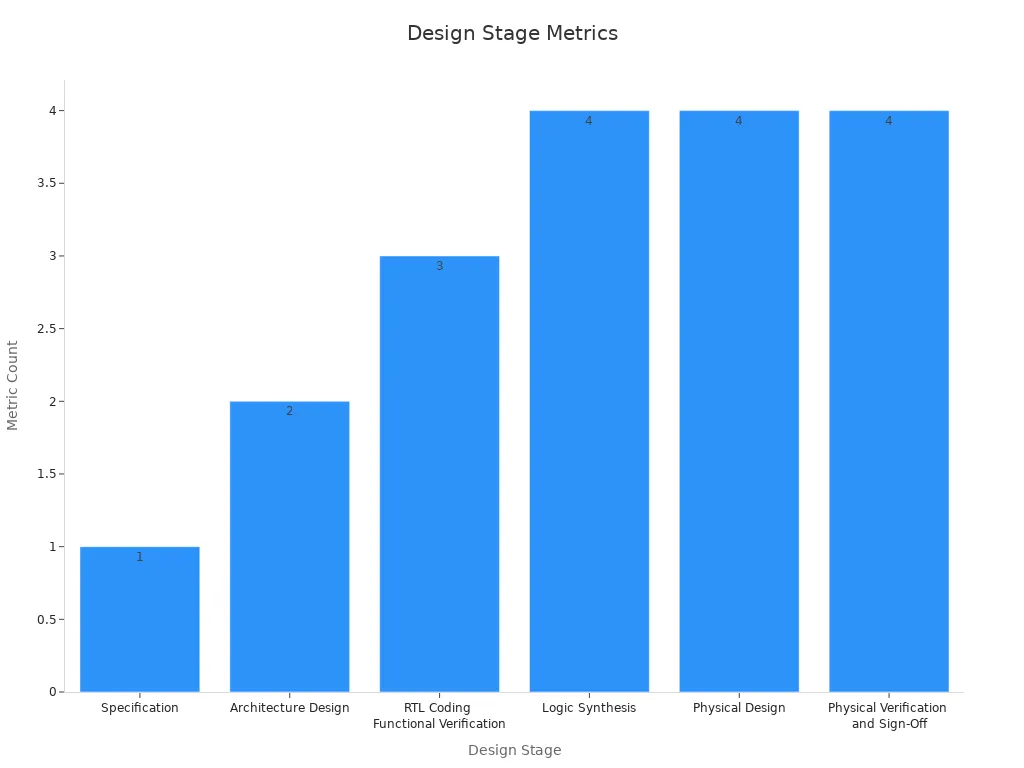
A well-defined architectural plan ensures the design flow remains efficient and reduces the risk of errors during later stages.
Schematic Design and Component Selection
After planning, engineers move to schematic design and component selection. They draw detailed circuit diagrams that show how each component connects. This step involves choosing transistors, resistors, capacitors, and other elements that match the required specifications. The design process at this stage focuses on accuracy and reliability.
Recent research highlights the use of reliability simulation tools, such as the BERT simulator, during schematic design. These tools predict degradation effects like hot electron impact, oxide breakdown, and electromigration. By simulating reliability early, engineers can improve performance prediction and reduce errors before fabrication. This approach increases the overall success rate of the integrated circuit design flow.
Tip: Early reliability simulation helps engineers catch potential failures before they become costly problems.
Layout and Physical Design Techniques
Layout and physical design techniques translate the schematic into a physical structure on silicon. Engineers use floorplanning, placement, and routing to arrange components and wires efficiently. The Mason global floorplanning approach, for example, combines mincut and slicing paradigms to create compact layouts and improve routability. This method uses a slicing-tree representation and in-place partitioning to speed up the design process.
A study comparing placement algorithms, such as Dragon, Capo, and QPlace, found that wirelength performance can range from 1.43 to 2.12 times the optimal value on average. As the number of modules increases, solution quality may drop by up to 17%. These findings show that layout techniques directly affect the efficiency and scalability of the integrated circuit design flow.
| Aspect | Details |
|---|---|
| Study Focus | Optimality and scalability of placement algorithms in IC design |
| Benchmark Size | 10k to 2M placeable modules |
| Algorithms Evaluated | Dragon, Capo, mPL, mPG (academic); QPlace (industrial) |
| Wirelength Performance | Worst case: 1.59 to 2.40 times optimal; Average: 1.43 to 2.12 times optimal |
| Scalability Impact | Solution quality deteriorates by 9% to 17% when problem size increases tenfold |
| Additional Findings | Effectiveness varies with circuit characteristics; nonlocal nets increase wirelength ratios |
Engineers must balance compactness, performance, and manufacturability during this stage. Efficient layout and physical design techniques help ensure the integrated circuit meets its performance and reliability goals.
Simulation, Verification, and Testing
Simulation, verification, and testing form the backbone of a robust integrated circuit design process. Engineers use simulation tools to check functionality, timing, power, and noise at different abstraction levels before fabrication. These tools help identify errors early, reducing costly mistakes later in the design flow. High-performance integrated circuits, such as microprocessors, often face electrical, mechanical, and thermal failures. Stability of device parameters remains essential for correct system function. Adjusting operational parameters like clock speeds can directly impact reliability and system lifetime.
Simulation platforms like Cadence Xcelium and Spectre provide scalable, high-accuracy verification across analog, digital, and mixed domains. Analog simulation offers the highest accuracy at the transistor level, while digital simulation delivers high performance and full verification flow. FastSPICE simulators partition transistor-level netlists for faster computation, balancing accuracy and speed. Design verification engineers benefit from DMS simulation, which runs faster than full AMS simulation but maintains verification fidelity.
Engineers use Design for Testability techniques, such as scan chains and built-in self-test, to improve test coverage and reliability. Post-silicon validation tests fabricated integrated circuits under real-world conditions, including voltage, temperature, and load. Debugging tools like logic analyzers and emulators provide visibility to isolate and fix faults. Verification plans define goals, strategies, and metrics to guide the process. Functional testing benchmarks, such as Automated Test Pattern Generation, improve test coverage and reduce verification time. Performance testing uses high-frequency simulation tools and in-circuit emulation platforms to optimize performance. Environmental testing, including thermal cycling and vibration, assesses durability. These steps ensure that integrated circuits meet functional correctness, performance targets, and reliability requirements.
Design Automation Tools and Software
Electronic design automation (EDA) tools and software have revolutionized the integrated circuit design process. These tools automate complex tasks, making the design flow more efficient and reliable. Engineers rely on EDA platforms for schematic capture, layout, simulation, and verification. Mixed-signal simulation platforms, such as Cadence Xcelium integrated with Spectre, enable high-accuracy verification across analog and digital domains. Modeling languages like SPICE and FastSPICE set benchmarks for analog IP verification accuracy.
Electronic design automation tools address critical challenges in integrated circuit design. They help minimize crosstalk by optimizing layout and ground planes. Clock signal skew reduction is achieved through trace length matching and impedance control. Thermal management benchmarks include efficient heat dissipation using thermal vias, copper planes, and advanced cooling methods. Durability benchmarks involve simulating mechanical and electrical stresses to predict material fatigue and ensure reliability.
Engineers use cloud-based transient thermal analysis to evaluate dynamic temperature and heat flux over time. Multiphysics simulation capabilities combine thermal and structural analysis, predicting hotspots and deformation. Functional testing benchmarks, such as portable stimulus models, improve test coverage and reduce verification time. Case studies show that Automated Test Pattern Generation can reduce verification time by 20%, while Palladium emulation improves core clock speed by 55%. These technological benchmarks confirm the effectiveness of simulation and verification tools within the design process. Electronic design automation software continues to drive innovation, enabling engineers to create reliable, high-performance integrated circuits.
Modern Applications of Integrated Circuits

Consumer Electronics and Smart Devices
Integrated circuits drive innovation in consumer electronics and smart devices. Microcontrollers manage device functions in smartphones, wearables, and home appliances. Memory and logic ICs support data storage and complex processing, enabling features like artificial intelligence and seamless connectivity. Analog ICs handle power management and wireless communication, which are essential for energy efficiency and performance. In smart homes, wireless communication ICs connect devices to networks, while sensor ICs detect environmental changes and automate responses. Power management ICs optimize energy use, making devices more efficient and reliable. These advancements highlight how integrated circuits serve as the backbone of smart device technology, supporting rapid growth in this sector.
Automotive Integrated Circuit Design
Automotive design relies on integrated circuits for safety, efficiency, and advanced features. Modern vehicles use ICs for engine control, infotainment, and driver assistance systems. Quality control processes ensure reliability and safety. Tools must meet ISO 26262 standards, and designers use fault modeling and injection testing to anticipate failures. Safety mechanisms like error correction codes and redundancy protect against faults. Verification methods, including simulation and hardware emulation, validate ICs for Automotive Safety Integrity Levels. Documentation and traceability support compliance throughout the product lifecycle. Stress test qualifications, such as AEC-Q100, confirm IC reliability across temperature ranges. These practices make integrated circuits essential for automotive applications, supporting autonomous driving and enhanced safety.
Medical Device Applications
Medical device applications depend on integrated circuits for accuracy, reliability, and patient safety. Clinical metrics, such as vital signs monitoring, use ICs to deliver individualized care. Early warning systems and machine learning techniques improve alarm accuracy and reduce false alerts. Wireless monitoring supports remote patient care and integration with electronic health records. ISO 13485 certification ensures quality control and traceability, while hardware security and error correction features enhance reliability. Compliance with safety standards and validated software designs simplify certification. Reliable data quality metrics and machine learning classifiers improve trust in AI-based monitors. Integrated circuits enable advanced medical applications, supporting continuous innovation in healthcare technology.
Industrial Automation and Control Systems
Industrial automation and control systems rely heavily on integrated circuits to achieve efficiency, accuracy, and safety. These systems use sensors, controllers, and actuators to monitor and manage industrial processes. Integrated circuits play a central role in the design of programmable logic controllers (PLCs), motor drives, and industrial robots. Engineers select specific ICs to handle tasks such as signal processing, data conversion, and real-time control.
Factories use automation to increase productivity and reduce human error. Integrated circuits enable fast response times and precise measurements. For example, analog-to-digital converters (ADCs) transform sensor signals into digital data for processing. Microcontrollers execute control algorithms that adjust machinery based on sensor feedback. Power management ICs ensure stable operation even in harsh environments.
Note: Reliable circuit design helps prevent costly downtime and equipment failure in industrial settings.
Industrial automation benefits from the miniaturization of integrated circuits. Smaller components allow for compact control panels and distributed control systems. Engineers can now embed advanced features like predictive maintenance and machine learning directly into industrial equipment.
The table below highlights common applications of integrated circuits in industrial automation:
| Application Area | Integrated Circuit Role |
|---|---|
| Process Control | Real-time monitoring and adjustment |
| Robotics | Motor control and sensor integration |
| Power Management | Voltage regulation and protection |
| Safety Systems | Fault detection and emergency response |
Engineers continue to improve the design of industrial automation systems by integrating more functions onto single chips. This trend supports smarter factories and more flexible manufacturing processes. Integrated circuits remain essential for the reliable and efficient operation of modern industrial applications.
Robust design principles and methodologies drive progress in technology. The design process supports innovation, reliability, and efficiency across many industries. Recent studies show that collaboration and support organizations boost innovation outcomes, as seen in the table below.
| Aspect | Key Finding |
|---|---|
| Innovation | Collaboration increases exploratory innovation |
| Industry Impact | Broad applicability across high-tech industries |
Market projections indicate strong growth, with the integrated circuit design service market expected to nearly double by 2033. Advances in AI, chiplet technology, and sustainable practices will shape the future of design.
FAQ
What is the main goal of integrated circuit design?
Engineers aim to create circuits that balance performance, power efficiency, and reliability. They use advanced tools and methods to ensure each chip meets specific requirements for its intended application.
How do engineers test integrated circuits before production?
Engineers use simulation and verification tools to check circuit behavior. They run tests for timing, power, and signal integrity. These steps help catch errors early and improve the final product’s quality.
Why is miniaturization important in integrated circuits?
Miniaturization allows engineers to fit more functions into smaller chips. This process leads to faster, more efficient devices. It also reduces manufacturing costs and supports the development of compact electronics.
What role do integrated circuits play in medical devices?
Integrated circuits power sensors, monitors, and control systems in medical devices. They help deliver accurate data and reliable performance. These features support patient safety and enable advanced healthcare technology.
Written by Jack from AIChipLink.
AIChipLink, one of the fastest-growing global independent electronic components distributors in the world, offers millions of products from thousands of manufacturers, and many of our in-stock parts is available to ship same day.
We mainly source and distribute integrated circuit (IC) products of brands such as Broadcom, Microchip, Texas Instruments, Infineon, NXP, Analog Devices, Qualcomm, Intel, etc., which are widely used in communication & network, telecom, industrial control, new energy and automotive electronics.
Empowered by AI, Linked to the Future. Get started on AIChipLink.com and submit your RFQ online today!


