Quick Reference: 7404 IC Basics
What is 7404?
- Type: Hex Inverter (NOT gate)
- Gates: 6 independent inverters
- Family: 74xx TTL logic
- Package: 14-pin DIP
- Voltage: 5V DC
- Speed: 10 ns typical propagation delay
Quick Answer: 7404 is a digital logic IC containing 6 NOT gates (inverters). Input HIGH → Output LOW, Input LOW → Output HIGH.
Understanding the 7404 IC
What Does 7404 Do?
Simple Explanation: The 7404 inverts (reverses) digital signals.
Input  → 7404 → Output
HIGH   →  IC  → LOW
LOW    →  IC  → HIGH
1      →  IC  → 0
0      →  IC  → 1
Analogy: Like a "reverse switch" - when you turn it ON, it outputs OFF.
Truth Table
| Input (A) | Output (Y) |
|---|---|
| 0 (LOW) | 1 (HIGH) |
| 1 (HIGH) | 0 (LOW) |
Logic Symbol:
     ┌─────┐
A ───┤  ○  ├─── Y
     └─────┘
      NOT
     (Inverter)
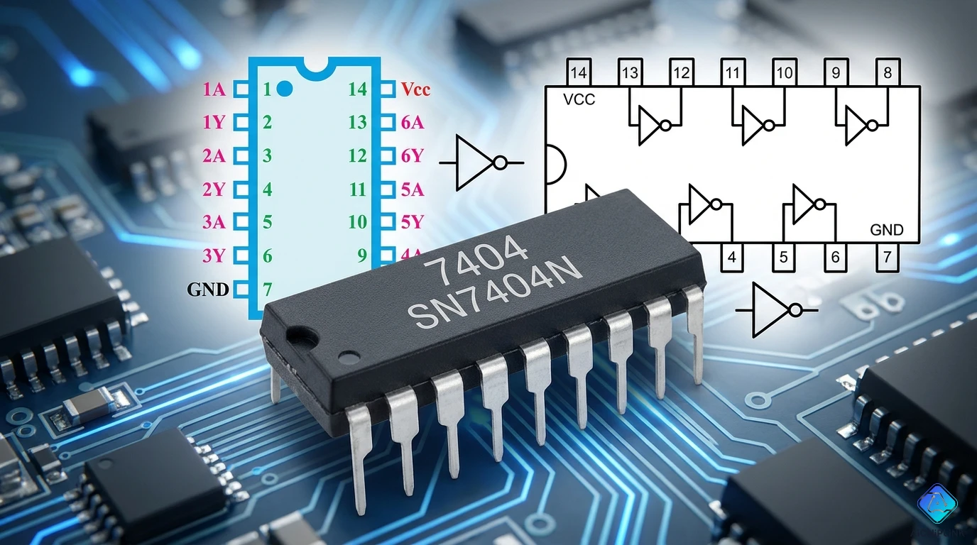
Pinout Diagram
14-Pin DIP Package
        7404 IC Top View
        ┌────────────┐
  1A ─┤ 1        14 ├─ VCC (+5V)
  1Y ─┤ 2        13 ├─ 6A
  2A ─┤ 3        12 ├─ 6Y
  2Y ─┤ 4        11 ├─ 5A
  3A ─┤ 5        10 ├─ 5Y
  3Y ─┤ 6         9 ├─ 4A
 GND ─┤ 7         8 ├─ 4Y
        └────────────┘
Pin Functions
| Pin | Name | Function |
|---|---|---|
| 1 | 1A | Inverter 1 Input |
| 2 | 1Y | Inverter 1 Output |
| 3 | 2A | Inverter 2 Input |
| 4 | 2Y | Inverter 2 Output |
| 5 | 3A | Inverter 3 Input |
| 6 | 3Y | Inverter 3 Output |
| 7 | GND | Ground (0V) |
| 8 | 4Y | Inverter 4 Output |
| 9 | 4A | Inverter 4 Input |
| 10 | 5Y | Inverter 5 Output |
| 11 | 5A | Inverter 5 Input |
| 12 | 6Y | Inverter 6 Output |
| 13 | 6A | Inverter 6 Input |
| 14 | VCC | Power (+5V) |
Key Points:
- All 6 inverters are independent
- Pin 7 = GND (must connect!)
- Pin 14 = VCC (+5V power)
- Inputs = odd pins (except 7,14)
- Outputs = even pins (except 7,14)
Technical Specifications
Electrical Characteristics
Supply Voltage (VCC):
- Recommended: 5V ±5% (4.75V - 5.25V)
- Absolute maximum: 7V
- Minimum: 4.5V
Input Voltage (VIN):
- HIGH (logic 1): 2.0V - 5.5V
- LOW (logic 0): 0V - 0.8V
- Never exceed VCC + 0.5V!
Output Voltage (VOUT):
- HIGH (VOH): 2.4V min @ 0.4mA
- LOW (VOL): 0.4V max @ 16mA
Current:
- Input current: 40 µA typical
- Output current: 16mA max per gate
- Total power: 33 mW per gate
Speed:
- Propagation delay (tpd): 10 ns typical
- Rise time (tr): 12 ns
- Fall time (tf): 8 ns
Common Problems & Troubleshooting
Problem 1: Output Always HIGH (Won't Go LOW) ⚠️
Symptoms:
- Output stuck at ~5V regardless of input
- No signal inversion occurring
Diagnostic Steps:
Step 1: Check Power Supply
Multimeter Test:
1. Set meter to DC voltage
2. Measure Pin 14 (VCC): Should be 4.75V - 5.25V
3. Measure Pin 7 (GND): Should be 0V
4. Voltage difference: Should be ~5V

❌ If wrong voltage → Fix power supply first
Step 2: Check Output Load
Problem: Output overloaded (too much current)
Test: Disconnect load from output pin
If works now → Load draws >16mA (exceeds spec)

Solution:
- Add buffer transistor (2N3904)
- Use 7407 (open-collector) instead
- Add current-limiting resistor
Step 3: Test IC with Minimal Circuit
Simple Test Setup:
VCC (Pin 14) → +5V
GND (Pin 7)  → Ground
Input (Pin 1) → Connect to GND (LOW)
Output (Pin 2) → Should read ~5V (HIGH)

Then:
Input (Pin 1) → Connect to VCC (HIGH)
Output (Pin 2) → Should read ~0V (LOW)

❌ If output stays HIGH → IC damaged, replace
Common Causes:
- ✅ Damaged IC (replace)
- ✅ Output pin shorted to VCC
- ✅ Excessive load current
- ✅ Latch-up from voltage spike
Problem 2: Output Always LOW (Won't Go HIGH) ⚠️
Symptoms:
- Output stuck at ~0V regardless of input
- Inverted signal not appearing
Diagnostic Steps:
Step 1: Check for Short to Ground
Power OFF test:
1. Remove IC from circuit
2. Use multimeter continuity mode
3. Check output pin to ground
4. Should be OPEN (no continuity)

❌ If continuity exists → PCB trace shorted
Step 2: Check Input State
Problem: Input floating (undefined state)
Measure input voltage with multimeter

If between 0.8V - 2.0V:
→ Input in "forbidden zone" (undefined)
→ IC behavior unpredictable

Solution:
- Add pull-up resistor (10kΩ to VCC) OR
- Add pull-down resistor (10kΩ to GND)
- Ensure input always driven HIGH or LOW
Step 3: Verify IC Not Reversed
Check IC orientation:
Look for notch or dot on Pin 1

Correct orientation:
  Notch/Dot
      ↓
  ┌───────┐
→ │ 1  14 │ ←
  │ 2  13 │

❌ If reversed → Remove immediately (may be damaged)
Common Causes:
- ✅ Output shorted to ground
- ✅ Floating input (undefined state)
- ✅ IC inserted backwards
- ✅ Damaged IC
Problem 3: IC Gets Hot 🔥
Symptoms:
- IC too hot to touch (>60°C)
- Rapid heating after power on
- Burning smell
IMMEDIATE ACTION: Power OFF immediately!
Diagnostic Steps:
Step 1: Check Supply Voltage
Measure VCC with multimeter:
- Should be 5V ±5%
- If >7V → Immediately disconnect!

Overvoltage damage:
6V: Reduced life
7V: Maximum rating
>7V: Permanent damage occurs
Step 2: Check for Shorts
Power OFF, IC removed:
1. Check VCC to GND resistance
2. Should be >1kΩ minimum
3. <100Ω indicates short circuit

Common short locations:
- Solder bridges between pins
- Damaged PCB traces
- Shorted capacitors
Step 3: Check Current Draw
Normal current per IC: ~60mA total
Measure with ammeter in VCC line

If >100mA:
→ Short circuit or latch-up
→ Do NOT continue powering

If <60mA but still hot:
→ One gate damaged (replace IC)
Common Causes:
- ✅ Excessive voltage (>5.25V)
- ✅ Short circuit (VCC to GND)
- ✅ Output driving too much current
- ✅ Latch-up condition
- ✅ Reverse polarity connection
Solutions:
1. Add 100µF capacitor across VCC-GND (reduce noise)
2. Add current-limiting resistor (220Ω in VCC line)
3. Use regulated 5V supply (not raw battery)
4. Add flyback diode if driving inductive loads
Problem 4: Intermittent Operation ⚡
Symptoms:
- Works sometimes, fails randomly
- Glitches in output signal
- Noise-sensitive behavior
Diagnostic Steps:
Step 1: Check Decoupling Capacitor
Critical: 0.1µF ceramic capacitor needed!
Location: Pin 14 (VCC) to Pin 7 (GND)
Distance: Within 0.5 inches of IC

Without decoupling:
- Power supply noise couples into IC
- High-frequency glitches occur
- Unreliable operation

Solution: Add 0.1µF ceramic cap (mandatory)
Step 2: Check Input Signal Quality
Use oscilloscope to inspect input:
Look for:
- Clean edges (sharp transitions)
- No ringing or oscillations
- Proper voltage levels (0V or 5V)

Problems to fix:
- Slow rise time → Add Schmitt trigger (74HC14)
- Ringing → Add small series resistor (100Ω)
- Noise → Add input filter capacitor (100pF)
Step 3: Check Grounding
All grounds must be common:
- Signal ground
- Power supply ground
- IC ground (Pin 7)

Test: Measure voltage between grounds
Should be <0.1V

If >0.1V → Ground loop problem
Fix: Star grounding topology
Common Causes:
- ✅ Missing decoupling capacitor
- ✅ Poor grounding
- ✅ Noisy power supply
- ✅ Loose connections
- ✅ Damaged IC socket
Problem 5: Slow Switching Speed 🐌
Symptoms:
- Output changes slowly (not instant)
- Rounded edges on scope
- Reduced maximum frequency
Diagnostic Steps:
Step 1: Check Load Capacitance
Problem: Too much capacitance on output
Measure with LCR meter

TTL output can drive:
- 15pF typical
- 50pF maximum (with degraded speed)
- >50pF → Use buffer (7407)

Long PCB traces add capacitance:
1 inch trace ≈ 2-3pF
10 inch trace ≈ 20-30pF

Solution: Keep traces short!
Step 2: Check Pull-up Resistor Value
If using pull-up resistor:
- 1kΩ → Very slow (avoid)
- 2.2kΩ → Moderate speed
- 4.7kΩ → Good compromise
- 10kΩ → Faster, but weaker

Formula: tr = 2.2 × R × C
Where:
tr = rise time
R = pull-up resistance
C = load capacitance

Example: 10kΩ, 20pF → tr = 440ns
Step 3: Verify IC Variant
Different 7404 families:
- 7404 (Standard TTL): 10ns
- 74LS04 (Low-power): 15ns (slower)
- 74HCT04 (CMOS): 8ns (faster)
- 74F04 (Fast): 3ns (fastest)

Check IC marking! May have wrong variant.
Testing Procedures
Basic Functionality Test
Equipment Needed:
- Multimeter
- LED + 330Ω resistor
- +5V power supply
Test Circuit:
        +5V
         │
         ├──────────── Pin 14 (VCC)
         │
      [Switch]
         │
         ├──────────── Pin 1 (Input)
         │
        GND
         │
         ├──────────── Pin 7 (GND)

    Pin 2 (Output)
         │
        [330Ω]
         │
        [LED]
         │
        GND

Test:
Switch OPEN (Input LOW) → LED should be ON (Output HIGH)
Switch CLOSED (Input HIGH) → LED should be OFF (Output LOW)
Propagation Delay Test
Equipment: Oscilloscope (dual-channel)
Procedure:
1. Apply 1 MHz square wave to input (Pin 1)
2. Connect scope:
   - Ch1: Input signal
   - Ch2: Output signal (Pin 2)
3. Measure time difference between edges
4. Typical delay: 10ns (7404), 3ns (74F04)

If delay >20ns:
→ IC may be damaged or wrong variant
Current Sourcing/Sinking Test
Test Output HIGH Current (Sourcing):
Setup:
Pin 2 (Output) → [1kΩ resistor] → GND
Pin 1 (Input) → GND (to make output HIGH)

Measure voltage at output:
Should be >2.4V (meets VOH spec)

If <2.4V → IC weak, consider replacement
Test Output LOW Current (Sinking):
Setup:
Pin 2 (Output) → [330Ω resistor] → +5V
Pin 1 (Input) → +5V (to make output LOW)

Measure voltage at output:
Should be <0.4V (meets VOL spec)

Calculate current: I = (5V - 0.4V) / 330Ω ≈ 14mA
Should handle up to 16mA
Troubleshooting Flowchart
START: 7404 Not Working Properly
│
├─ Symptom: Output always HIGH?
│  ├─ Check power: VCC = 5V?
│  │  ├─ NO → Fix power supply
│  │  └─ YES → Continue
│  ├─ Check load: Disconnect load, works now?
│  │  ├─ YES → Reduce load current
│  │  └─ NO → Replace IC (damaged)
│
├─ Symptom: Output always LOW?
│  ├─ Check for short: Output to GND?
│  │  ├─ YES → Fix short circuit
│  │  └─ NO → Continue
│  ├─ Check input: Voltage in 0.8V-2.0V range?
│  │  ├─ YES → Add pull-up or pull-down
│  │  └─ NO → Check IC orientation
│     └─ Reversed? → Remove, check, reinstall
│
├─ Symptom: IC gets hot?
│  ├─ IMMEDIATE: Power OFF
│  ├─ Check voltage: >7V?
│  │  ├─ YES → Reduce to 5V
│  │  └─ NO → Continue
│  ├─ Check current: >100mA?
│  │  ├─ YES → Find short circuit
│  │  └─ NO → Replace IC
│
├─ Symptom: Intermittent operation?
│  ├─ Add 0.1µF cap: Pin 14 to Pin 7
│  ├─ Check grounding: Common ground?
│  ├─ Check input signal: Clean edges?
│  └─ Tighten connections
│
└─ Symptom: Slow switching?
   ├─ Check load: <50pF?
   ├─ Reduce trace length
   ├─ Check IC variant: Standard 7404?
   └─ Consider faster variant (74F04)
Alternative ICs & Cross-Reference
Direct Replacements
| Part Number | Family | Speed | Notes |
|---|---|---|---|
| 7404 | TTL | 10ns | Standard |
| 74LS04 | LS-TTL | 15ns | Lower power, slower |
| 74ALS04 | ALS-TTL | 8ns | Low power, fast |
| 74F04 | Fast TTL | 3ns | Fastest TTL |
| 74HCT04 | CMOS | 8ns | CMOS, TTL compatible ⭐ |
| 74HC04 | CMOS | 8ns | CMOS only (3.3V-5V) |
| CD4049 | CMOS | 50ns | Can level-shift |
Best Modern Alternative: 74HCT04 (CMOS, faster, lower power)
Pin-Compatible Equivalents
All these ICs have identical 14-pin pinout:
- SN7404 (Texas Instruments)
- DM7404 (National Semiconductor)
- HD7404 (Hitachi)
- MC7404 (Motorola)
- µPB7404 (NEC)
All are interchangeable!
Practical Applications
Application 1: Signal Inversion
Problem: Need to reverse logic signal
Solution:
      Input              7404          Output
        │                 │              │
    [Signal] ──────► Pin 1     Pin 2 ──► [Inverted]
                      │                   Signal
                    Pin 14
                      │
                     +5V
Example: LED ON when button NOT pressed
Application 2: Crystal Oscillator Buffer
Circuit:
    Crystal (10MHz)
         │
         ├────[10MΩ]────┐
         │              │
      Pin 1          Pin 2
      (7404)         (7404)
         │              │
         └──────────────┘

Output from Pin 2: 10 MHz square wave
Application 3: Level Shifter (Using CD4049)
5V to 3.3V Conversion:
5V Logic ──► CD4049 ──► 3.3V Logic
            (VCC=3.3V)
Note: Standard 7404 cannot do this, use CD4049 instead.
Application 4: Make NAND Gate from Inverters
Two inverters + wired-AND:
A ──►│ │──┐
      │ │  └───── Output
B ──►│ │──┘
      7404

Truth Table:
A B | Out
0 0 | 1
0 1 | 1
1 0 | 1
1 1 | 0  (NAND function)
Design Guidelines
PCB Layout Best Practices
Power Decoupling:
Critical: 0.1µF ceramic capacitor
Placement: <0.5 inch from IC
Between: Pin 14 (VCC) and Pin 7 (GND)

Additional: 10µF electrolytic at power entry point
Trace Routing:
Signal traces:
- Keep short (<6 inches if possible)
- Avoid long parallel runs (crosstalk)
- 50Ω impedance if >1 MHz

Power traces:
- Wide traces for VCC and GND
- Minimum 20 mil width for 100mA
Grounding:
Star grounding:
     Power Supply Ground
            │
            ├─── IC Ground (Pin 7)
            ├─── Signal Ground
            └─── Chassis Ground

Avoid: Daisy-chain grounding
Input Protection
For noisy environments:
Input ──[100Ω]──┬──► IC Pin
                │
              [100pF]
                │
               GND

RC filter: Cuts high-frequency noise
For ESD protection:
Input ──[1kΩ]──┬──► IC Pin
               │
            [Diode]
               │
              VCC
               │
            [Diode]
               │
              GND
Common Mistakes to Avoid
Mistake 1: Leaving Unused Inputs Floating ❌
Problem: Undefined state causes unpredictable behavior
Solution:
Unused inputs must be:
- Tied to GND (LOW) OR
- Tied to VCC through 10kΩ resistor (HIGH)

Never leave unconnected!
Mistake 2: Exceeding Output Current ❌
Problem: Each gate limited to 16mA
Bad:
Output ──[LED + 100Ω]── GND
Current = 5V / 100Ω = 50mA ❌ Too much!
Good:
Output ──[LED + 330Ω]── GND
Current = 5V / 330Ω = 15mA ✅ Safe
Mistake 3: Missing Decoupling Capacitor ❌
Consequence:
- Erratic operation
- Noise sensitivity
- Possible latch-up
Fix: Always use 0.1µF ceramic cap on every IC
Summary & Quick Tips
Key Takeaways
✅ 7404 = 6 independent inverters (NOT gates)
✅ Always use 5V power (4.75V - 5.25V range)
✅ Decoupling cap is mandatory (0.1µF ceramic)
✅ Max output current = 16mA per gate
✅ Never leave inputs floating (tie HIGH or LOW)
✅ Check IC orientation (notch/dot = Pin 1)
Troubleshooting Quick Checks
- ☐ Power supply = 5V?
- ☐ Decoupling cap present?
- ☐ IC oriented correctly?
- ☐ No shorts between pins?
- ☐ Output load <16mA?
- ☐ Inputs not floating?
Conclusion
The 7404 hex inverter is a fundamental building block of digital logic, offering six independent NOT gates in a single package. While simple in function, proper troubleshooting requires systematic checks of power supply, signal integrity, and load conditions.
Most Common Issues (80% of problems):
- Missing decoupling capacitor
- Floating inputs
- Excessive output current
- Wrong supply voltage
For more IC tutorials, troubleshooting guides, and electronics resources, visit AiChipLink.com.

Written by Jack Elliott from AIChipLink.
AIChipLink, one of the fastest-growing global independent electronic components distributors in the world, offers millions of products from thousands of manufacturers, and many of our in-stock parts is available to ship same day.
We mainly source and distribute integrated circuit (IC) products of brands such as Broadcom, Microchip, Texas Instruments, Infineon, NXP, Analog Devices, Qualcomm, Intel, etc., which are widely used in communication & network, telecom, industrial control, new energy and automotive electronics.
Empowered by AI, Linked to the Future. Get started on AIChipLink and submit your RFQ online today!
Frequently Asked Questions
What is the 7404 IC used for?
The 7404 IC is primarily used for signal inversion in digital circuits, meaning it converts logic HIGH to LOW and vice versa. It is commonly applied in clock signal shaping, waveform generation, logic control, and interfacing between circuit stages where inverted logic is required.
Can I use the 7404 IC with 3.3V systems?
The standard 7404 IC is designed for 5V TTL operation and does not reliably work at 3.3V. For 3.3V systems, you should use CMOS alternatives like 74HC04 or 74HCT04, which offer better compatibility and lower power consumption.
Why is my 7404 output unstable or noisy?
Unstable output is usually caused by missing decoupling capacitors, floating inputs, or poor grounding. The 7404 IC requires a 0.1µF capacitor between VCC and GND and all unused inputs must be tied HIGH or LOW to prevent unpredictable switching.
How much current can a 7404 output drive?
Each gate in the 7404 IC can sink up to about 16mA and source significantly less current. Exceeding this limit can cause voltage drop, incorrect logic levels, or even permanent damage, so external drivers or buffers are recommended for higher loads.
What are the best modern replacements for 7404?
Modern designs often replace the 7404 IC with CMOS variants like 74HCT04 or 74F04, which provide faster switching, lower power consumption, and better noise immunity depending on the application requirements.


.png&w=256&q=75)


