In the world of electronics, the packaging of integrated circuits (ICs) is critical. One of the most widely used forms of IC packaging is the Dual Inline Package (DIP). Understanding the structure, purpose, and applications of the DIP package can help individuals and companies make informed decisions when sourcing or utilizing semiconductor components. This article will provide an in-depth explanation of the DIP package, including its components, variations, and practical applications.
What is a Dual Inline Package (DIP)?
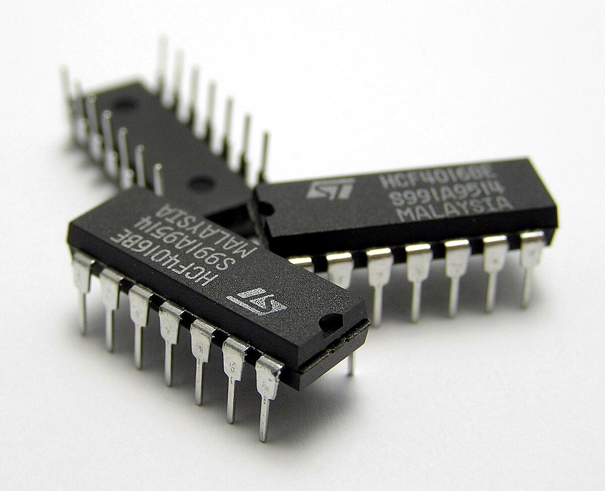
A Dual Inline Package (DIP) is a type of electronic component packaging used for ICs and other semiconductor devices. The name "dual inline" refers to the package's layout, where the pins are arranged in two parallel rows on either side of the component. This packaging format is one of the oldest and most recognized methods for mounting and connecting ICs to printed circuit boards (PCBs).
The DIP package is typically used for small to medium-sized electronic components, such as microcontrollers, logic chips, and memory ICs. It has been widely utilized in various applications, from consumer electronics to industrial machinery.
Key Features of the DIP Package
1. Two Parallel Rows of Pins: The most distinct characteristic of a DIP is its two rows of pins. The number of pins can range from as few as 4 to as many as 64, depending on the size and complexity of the IC.
2. Through-Hole Mounting: DIP components are designed to be inserted into holes in a PCB, a process known as through-hole technology (THT). The pins are inserted into the PCB's holes, and the component is soldered in place, providing a stable connection.
3. Durability and Reliability: DIP components are known for their durability. The robust pins and through-hole mounting ensure a solid mechanical connection, making them suitable for environments with high vibration or electrical interference.
4. Large Form Factor: Compared to modern surface-mount packages like SMD (Surface-Mount Devices), DIPs have a larger form factor. This makes them easier to handle and replace, particularly in prototyping and repair scenarios.
Types of Dual Inline Packages
There are several types of DIP packages based on the number of pins, size, and function of the IC. Some of the most common types include:
• Standard DIP: This is the typical form of the DIP package, featuring two rows of pins on either side of the component.
• Small Outline DIP (SODIP): A more compact version of the standard DIP, designed for smaller and thinner ICs.
• Plastic Dual Inline Package (PDIP): This is the most common type, where the component is enclosed in a plastic casing, offering excellent protection and insulation.
• Ceramic Dual Inline Package (CDIP): A more robust variation where the casing is made from ceramic, providing better heat resistance and performance in extreme conditions.
Advantages of DIP Packaging
1. Ease of Use: DIPs are very easy to handle and work with. Their large size makes them ideal for prototyping and debugging in laboratories and workshops.
2. Repairability: Unlike modern surface-mount components, which require specialized equipment for soldering and desoldering, DIPs can be easily replaced or reworked manually, making them ideal for repair work.
3. Availability: The DIP package has been in use for decades, and its widespread use ensures that replacement parts are readily available for various applications.
4. Cost-Effective: Due to its simplicity in design and long history of use, DIP components are often more cost-effective than more modern packaging options like QFP (Quad Flat Package) or BGA (Ball Grid Array).
5. Stability: DIPs are reliable and provide a stable connection, making them ideal for high-power and high-frequency applications.
Disadvantages of DIP Packaging
1. Size: DIPs are significantly larger than surface-mount packages, making them unsuitable for high-density PCBs where space is at a premium.
2. Limited Pin Count: While there are DIPs with as many as 64 pins, they are still limited compared to modern packages, which can offer hundreds or even thousands of pins in smaller form factors.
3. Manual Assembly: Since DIPs use through-hole mounting, they require more manual labor during assembly, especially for high-volume production runs. This can increase the overall manufacturing cost.
DIP Package vs. Surface-Mount Devices (SMD)
| Feature | Dual Inline Package (DIP) | Surface-Mount Device (SMD) |
|---|---|---|
| Size | Larger, through-hole component | Smaller, directly mounted on the PCB |
| Pin Count | Typically 4 to 64 pins | Can be in the hundreds or more |
| Assembly Process | Through-hole soldering | Surface-mount soldering (requires specialized equipment) |
| Ease of Repair | Easier to replace and repair manually | More difficult to repair manually |
| Use Case | Prototyping, repair, and low-density PCBs | High-density and mass production PCBs |
| Cost | Generally cheaper | More expensive due to automation and smaller sizes |
| Performance | Suitable for low-to-moderate power | Optimized for high-speed and low-power consumption |
Applications of the DIP Package
The DIP package has been used extensively in various sectors and applications:
1. Consumer Electronics: Many early electronic devices, such as TVs, radios, and computers, utilized DIP packages for ICs due to their ease of use and reliability.
2. Microcontrollers: DIP packages are common in microcontroller-based projects, particularly for hobbyists and in educational settings.
3. Memory Devices: Early memory chips, such as RAM and ROM, were often packaged in DIP formats.
4. Communication Equipment: DIP packages are used in communication systems that require durable and easy-to-replace components.
5. Automotive Electronics: In some automotive systems, especially older ones, DIPs can be found in components such as microprocessors and controllers.
How to Identify a DIP Package
DIP components typically have the following markings:
1. Part Number: A unique identifier used to specify the IC.
2. Manufacturer's Logo: The symbol or name of the manufacturer.
3. Pin 1 Indicator: An arrow, dot, or notch indicates where pin 1 starts.
When inspecting a DIP, always ensure that the number of pins matches the specification for your particular application.
FAQ - Frequently Asked Questions about DIP
1. What is the difference between a DIP and a SIP (Single Inline Package)?
A Single Inline Package (SIP) has a single row of pins, whereas a Dual Inline Package (DIP) has two rows of pins. Both are through-hole components, but DIPs provide more pin connections for more complex ICs.
2. Can I use a DIP component in modern devices?
While DIPs are largely replaced by smaller packages in modern electronics, they are still used in specific applications, such as prototyping, low-volume production, and repair work. Additionally, DIP switches are still used in settings requiring user-configurable settings.
3. How do I solder a DIP component to a PCB?
Soldering a DIP component involves placing the component into the PCB's holes, aligning the pins with the respective holes, and then soldering each pin. It's important to use a proper technique to avoid cold solder joints.
4. Why is the DIP package still used in some industries?
DIPs are still favored for their ease of repair, robustness, and low cost in applications where space is not a primary concern. Additionally, their large size makes them easier to handle, making them ideal for prototyping or educational projects.
5. Can I replace a DIP component with a surface-mount device?
In most cases, yes, but it requires careful design changes. Surface-mount devices require different PCB layouts, including more precise soldering techniques. Therefore, replacing a DIP with an SMD often necessitates designing a new PCB.
Conclusion
The Dual Inline Package (DIP) remains one of the most reliable and accessible forms of semiconductor packaging. Despite the increasing popularity of smaller and more compact surface-mount packages, the DIP continues to serve critical roles in prototyping, low-volume production, and repair applications. Whether you are a hobbyist working on a DIY electronics project or an engineer sourcing components for industrial equipment, understanding the DIP's structure, advantages, and limitations will help you make better choices when selecting components for your designs.
Written by Icey Ye from AIChipLink.
AIChipLink, one of the fastest-growing global independent electronic component distributors in the world, offers millions of products from thousands of manufacturers. Whether you need assistance finding the right part or electronic components manufacturers for your design, you can contact us via phone, chat or e-mail. Our support team will answer your inquiries within 24 hours.
Disclaimer: This article is provided for general information and reference purposes only. The opinions, beliefs, and viewpoints expressed by the author of this article do not necessarily reflect the opinions, beliefs, and viewpoints of AIChipLink or official policies of AIChipLink.