D Flip-Flop Definition, Truth Table, and Applications
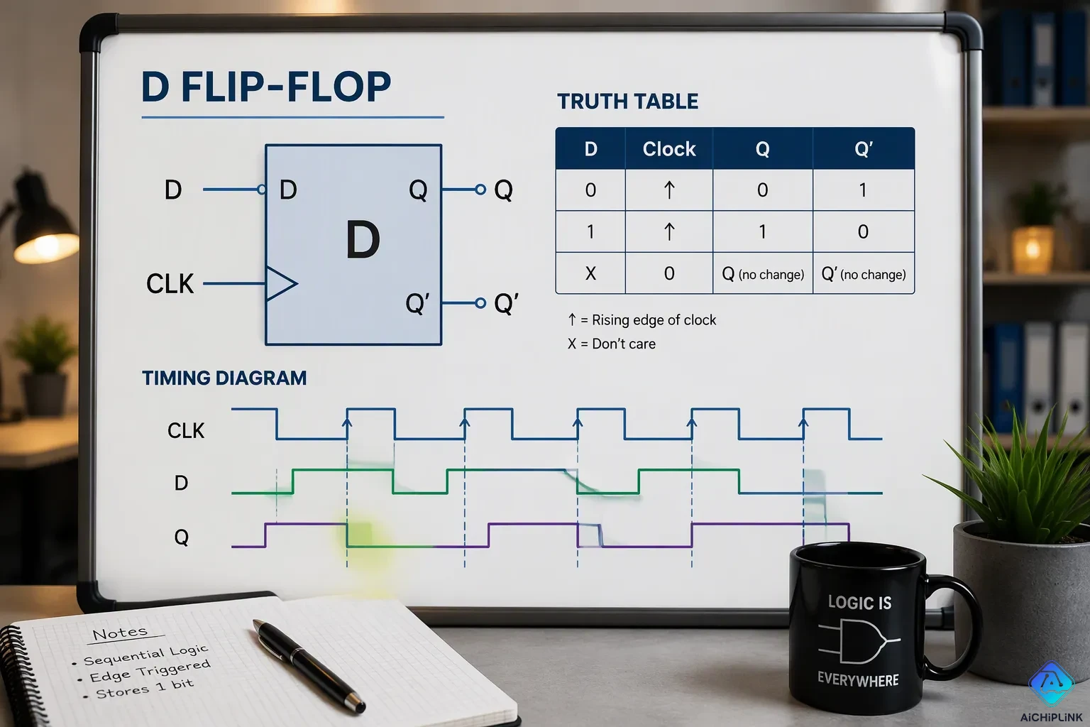
A D flip-flop is a one-bit digital memory element. It has one data input (D) and one clock input (CLK). When the clock edge comes, the circuit copies the value on D to the output Q. This simple step makes the d flip-flop a basic building block of digital storage.
Engineers depend on the D flip-flop because it holds data in a steady, predictable way. The d type flip-flop also gets rid of the invalid input state that causes problems in older latch designs. A d flip flop shows up in registers, counters, and control logic in many systems. This article explains how the d flip flop works, gives its truth table, and describes its real-world uses.
Key Takeaways
-
A D flip-flop stores one bit of data and copies the input to the output at the clock edge.
-
The truth table shows that the next output equals the D input when the clock edge arrives.
-
Edge-triggered D flip-flops prevent glitches and hold data steady between clock edges.
-
D flip-flops build registers, shift registers, and control logic in digital systems.
-
Low-power D flip-flops save energy and suit battery-powered devices.
What Is a D Flip-Flop
D Type Flip-Flop Definition
A d type flip-flop is a digital memory circuit. It can store one bit of data. The circuit has one data input (D) and one clock input (CLK). It also has two outputs: Q and its complement, Q̄. The d (data) flip-flop captures the value on D at the active clock edge. It holds that value at the q output until the next edge. Everything between edges is ignored. The stored bit survives as long as power stays on and the clock keeps running.
Engineers can build a d flip flop circuit from an SR flip-flop. They connect a NOT gate between the S and R inputs. They tie the two inputs together through that gate. The d input feeds the S input directly. The same d input passes through the NOT gate into the R input. This arrangement gives S = D and R = D'. The modified clocked SR flip-flop is known as the d flip-flop. The NOT gate guarantees that S and R never equal 1 at the same time. That guarantee is the main reason the design replaced the bare SR latch in synchronous systems. A d flip flop therefore offers a single, clean data path. A d flip-flop built this way is the standard cell in most logic libraries. Each d type flip-flop in a chain passes its stored value to the next stage.
D Flip-Flop Symbol and Inputs
The d flip-flop symbol shows a rectangle with labeled pins. The d input sits on the left side. The CLK input sits below it, marked with a small triangle. That triangle means the device is edge-triggered. The Q output and its complement appear on the right side. Many datasheets also label Preset and Clear pins, which set or reset the output directly. Pin names follow a common convention across vendors. D means data, CLK means clock, Preset forces Q to 1, and Clear forces Q to 0.
| Variant | Inputs | Outputs |
|---|---|---|
| Basic | D | Qnext, Q' |
| Gated (level-triggered) | CLK, D | Qnext, Q', Previous State |
| Rising-edge-triggered | CLK (rising edge), D | Qnext, Q', Previous State |
| Falling-edge-triggered | CLK (falling edge), D | Qnext, Q', Previous State |
| With Preset and Clear | CLK, D, Preset, Clear | Qnext, Q', Previous State |
A clear d flip-flop symbol helps readers trace signals quickly. The d flip-flop symbol always places the clock pin apart from the data pins. This layout reminds designers that D only matters at the edge. The symbol also shows the complement output, which many logic designs use. Designers who read the symbol correctly avoid wiring mistakes. A rising-edge device updates on the low-to-high transition. A falling-edge device updates on the high-to-low transition. The triangle alone does not tell which edge applies; the datasheet does. The d flip flop circuit then behaves as the truth table predicts. The d flip-flop holds its value until the next edge. Arrays of d flip-flops form registers, and those registers hold multi-bit values. Cascaded d flip-flops build shift registers.
How a D Flip-Flop Works
Clock Edge Operation
The d flip flop working follows a fixed sequence. A designer sets the d input to the wanted value while the clock stays low. The output Q does not change yet. The circuit waits for the active edge.
-
Set the d input to the desired value, such as 1, while the clock is low. Q keeps its old value.
-
Apply a rising edge to the clock, a transition from 0 to 1. The flip-flop samples D at that edge and copies it to Q.
-
Change D to a new value, such as 0, while the clock stays high. Q holds the captured value and shows the circuit is no longer transparent.
-
Away from the active edge, any change on D leaves Q untouched. The stored bit stays put.
A short pulse on D that falls entirely between rising edges is not captured. The d flip-flop: store the input data only when the sampling window overlaps the edge. Designers respect setup and hold time so the d input stays stable around that moment.
Q(t+1) = D
This relation means the value of Q after the next clock edge equals the value of D at that edge. The d flip-flop operation and applications rest on this one rule.
Edge-Triggered vs. Level-Triggered
A level-triggered D latch is transparent while enabled. Changes at D pass straight through to Q during that window. An edge-triggered device behaves differently. A positive edge-triggered d flip-flop samples D only at the rising transition. A negative edge-triggered d flip-flop samples at the falling transition.
| Feature | Level-triggered D latch | Edge-triggered D flip-flop |
|---|---|---|
| Response to control signal | Level-sensitive | Edge-sensitive |
| When data affects output | While enabled | Only at the active edge |
| Behavior between updates | Holds when disabled | Holds between edges |
The positive edge-triggered design suits synchronous systems. Several d flip-flops can share one clock and update together. The d flip flop therefore gives cleaner timing than a bare latch. A d flip flop also blocks brief glitches that a latch would pass. Teams pick the latch for simple transparent buffering and the d flip-flop for clocked storage.
D Flip-Flop Truth Table
Truth Table and Characteristic Equation
The d flip-flop truth table lists every clock condition next to the d input and the resulting output. Readers can check the behavior of the circuit in one glance.
| Clock Edge | D (Input) | Q (Next State) |
|---|---|---|
| Rising | 0 | 0 |
| Rising | 1 | 1 |
| No Edge | X | Q (No Change) |
The table shows three cases. A rising edge with a low d input drives Q to 0. A rising edge with a high d input drives Q to 1. The letter X marks a don't-care value. When no clock edge occurs, the output holds its previous state, no matter what happens on the d input. This hold row is the heart of the truth table of a d flip-flop. It explains why the device can store data between clock events.
A second version of the truth table of d flip-flop uses Q(n) and Q(n+1) labels. The rising edge copies D to the next output. The no-edge row keeps Q(n) unchanged. Both versions describe the same circuit, and either one works in a lab report or a design review.
The characteristic equation: Qn+1 = D states the same rule in one line. Qn+1 is the next state of the flip-flop. The next state always equals the d input at the active clock edge. The output therefore lags the input by one clock period. This delay gives the device its other name, the delay flip-flop. The truth table of a d flip-flop and the equation agree in every row, so students can use either tool to predict behavior.
Excitation Table and Timing
An excitation table works in the opposite direction. It starts with a wanted state change and asks what input produces it. To build one, list every combination of present state Q(t) and next state Q(t+1), then find the input value that forces the desired result.
| Present State Q(t) | Next State Q(t+1) | D Input |
|---|---|---|
| 0 | 0 | 0 |
| 0 | 1 | 1 |
| 1 | 0 | 0 |
| 1 | 1 | 1 |
The pattern is simple. The required d input equals the desired next state in every row. Designers use this table when they synthesize sequential logic. They pick the transitions they want, read the d input column, and wire the circuit to match.
Timing matters as much as logic. The d input must stay steady around the clock edge. A change too close to the edge can capture the wrong value. Engineers respect setup and hold times to keep the sample clean. Arrays of d flip-flops share one clock, so every stage updates at the same moment. This shared edge keeps multi-bit data aligned. The truth table predicts the logic, and timing rules make that prediction real in hardware.
Types, Advantages, and Limitations
Common Variations
The basic d flip flop comes in a few different versions. A gated, level-triggered type lets data pass through while the clock stays high. A rising-edge-triggered type takes a sample only on the low-to-high change. A falling-edge-triggered type takes its sample on the high-to-low change. Every version keeps the same single data input and the same way of holding a stored bit.
A d flip-flop with preset and clear adds two direct control pins. Preset pushes the output to 1, and clear pushes it to 0, without waiting for a clock edge. Designers use these pins to set a known starting state when power comes on. The d flip-flop circuit inside each variant uses the same NOT-gated SR core, so the logic stays familiar from part to part.
Advantages and Limitations
The d flip-flops give you a simple structure with only a few components. That simplicity makes it easy to fit them into ASICs and large systems. Edge triggering grabs input changes only at the clock edge, so the output stays steady for the rest of the cycle. A d flip flop also skips the invalid state that causes trouble in bare SR latches. Low-power designs cut consumption by charging and discharging only when needed.
| Advantages | Limitations |
|---|---|
| Single data input simplifies use and interfacing | No feedback path, so unsuitable for feedback control such as servo or motor loops |
| No feedback loop removes race conditions | Cannot toggle, since it responds to data, not the clock |
| No invalid or weak states | Propagation delay can cause timing issues in tight-timing systems |
| Bi-stable operation holds state until changed | Limited scalability; scaling up increases complexity and error potential |
The d flip-flop vs t flip-flop comparison shows where each one fits. A d flip-flop stores whatever value shows up on its data pin. A t flip-flop flips its output on every clock edge. The d flip-flop vs t flip-flop choice therefore depends on the job. Counters work best with the flipping behavior, and registers work best with the d type. The d flip-flop vs t flip-flop difference also matters in tight-timing designs, where the d type adds delay. Compact latch designs and improved cell counts cut down area when cost matters.
D Flip Flop Applications
Registers and Shift Registers
One d flip flop holds a single bit. Put several together and you get a register. Eight d flip-flops make an 8-bit register, which holds one byte. When each stage feeds the next, the group becomes a shift register. A shared clock moves the stored bits along, one stage per edge. With four stages, a bit needs four rising edges to go from input to output.
The four common layouts each fit a different job. A serial-in, serial-out register sends bits along one at a time. A serial-in, parallel-out version has an output pin at every stage, so data is ready before it reaches the last flip-flop. A parallel-in, serial-out register loads all bits at once and sends them out one by one. A parallel-in, parallel-out block is just a d flip-flop register with no chaining, and it gives its output within a single clock pulse. Ring and Johnson counters build on this idea by feeding the last output back to the first.
Control, Communication, and Low-Power Use
Communication systems count on these devices for conversion and alignment. Shift registers built from d flip-flops turn serial data into parallel words and back again. The same circuits keep sending and receiving in sync, so both ends agree on where each bit starts.
Counters and digital control logic also depend on the d flip flop. A ring counter repeats its pattern every four clock pulses with four stages, and a Johnson counter makes twice as many states as it has stages. Portable designs lower power with methods such as MTCMOS and output control, which can cut use by up to 53% without adding delay. Adiabatic designs report about 90% energy savings at 55.6 MHz. Product lines pair low power with propagation delay under 5 ns and a 0.8V–18V range. These traits explain the wide use of d flip-flop circuits in battery-powered equipment. One last use of d flip-flop logic shows up in memory interfacing, where the cell holds data until another block asks for it. All together, the applications of d flip-flop technology cover storage, control, and communication.
A d flip-flop is a one-bit memory element. It copies the value on D to Q at the clock edge. The truth table shows this behavior in every case. The characteristic equation, Q(next) = D, states the same rule in one line. Together, they let engineers predict the output before building the circuit.
The d type flip-flop plays a central role in digital design. Registers and shift registers use d flip-flops to store one bit of data per stage. Control logic, communication links, and low-power systems also rely on the d flip flop. Readers can now apply this understanding to their own designs.

Written by Jack Elliott from AIChipLink.
AIChipLink, one of the fastest-growing global independent electronic components distributors in the world, offers millions of products from thousands of manufacturers, and many of our in-stock parts is available to ship same day.
We mainly source and distribute integrated circuit (IC) products of brands such as Broadcom, Microchip, Texas Instruments, Infineon, NXP, Analog Devices, Qualcomm, Intel, etc., which are widely used in communication & network, telecom, industrial control, new energy and automotive electronics.
Empowered by AI, Linked to the Future. Get started on AIChipLink and submit your RFQ online today!
Frequently Asked Questions
What Does a D Flip-Flop Do?
It stores one bit. At the active clock edge, the d flip-flop copies the value on D to Q and holds it until the next edge. A d type flip-flop therefore acts as a simple one-bit memory cell in synchronous designs.
How to Test a D Flip-Flop in a Lab?
Read the d flip-flop symbol, then wire D and CLK to switches. Apply a rising edge with D low, then with D high. The output should follow. A logic probe confirms the hold state. Testing a d flip flop takes only a few steps.
How Do You Read a D Flip-Flop Truth Table?
The d flip-flop truth table lists D, the clock edge, and the next Q. A rising edge copies D to Q. With no edge, Q holds. The truth table makes this hold row easy to spot.
Where Do D Flip-Flops Fit Best?
Registers, shift registers, and control logic suit the d flip-flop well. Cascaded d flip-flops move bits one stage per clock. Engineers who know how to test a d flip-flop can verify each stage quickly.