Table of Contents
- 1.0 What is the AD7528LR? (Datasheet Explained)
- 1.1 The Classic Dual 8-Bit CMOS DAC
- 1.2 Decoding the "LR" Suffix
- 1.3 Key Specifications from the Datasheet
- 2.0 AD7528LR Pinout (SOIC-20 & PDIP-20)
- 2.1 20-Lead Package Pin Configuration
- 2.2 Pin Functions Explained (Data, Control, DAC I/O)
- 3.0 AD7528LR Applications and Use Cases
- 3.1 Digital-to-Analog Conversion for Microprocessors
- 3.2 Digitally Controlled Gain/Attenuation
- 3.3 Status as a Legacy Component
- 4.0 How to Use the AD7528LR: Interface & Design
- 4.1 Understanding the 8-Bit Microprocessor Interface
- 4.2 Basic Unipolar Operation Circuit
- 4.3 Finding an AD7528LR Equivalent or Replacement
- 5.0 Frequently Asked Questions (FAQ)
In today's world of 24-bit audio and 16-bit high-speed data converters, it’s easy to overlook the classics. But for engineers maintaining or repairing long-life industrial, medical, or audio equipment, legacy components are the lifeblood of their work. A perfect example is the AD7528LR Dual 8-Bit DAC. This chip was a cornerstone of 8-bit microprocessor systems in the 1980s and 90s, offering a compact and easy-to-use solution for getting two analog signals out of a digital system.
You won't find the AD7528LR in a 2025-era smartphone, but you will absolutely find it in test equipment, industrial controllers, and vintage synthesizers that are still in service today. The market for these mature components is driven by a critical need: you can't redesign a 20-year-old product, but you must be able to repair it.
This guide is for the engineer, technician, or supply chain manager who has this part in hand. We'll dive into the AD7528LR datasheet, explain its pinout, cover its most common applications, and discuss its status as a critical legacy component.
1.0 What is the AD7528LR? (Datasheet Explained)
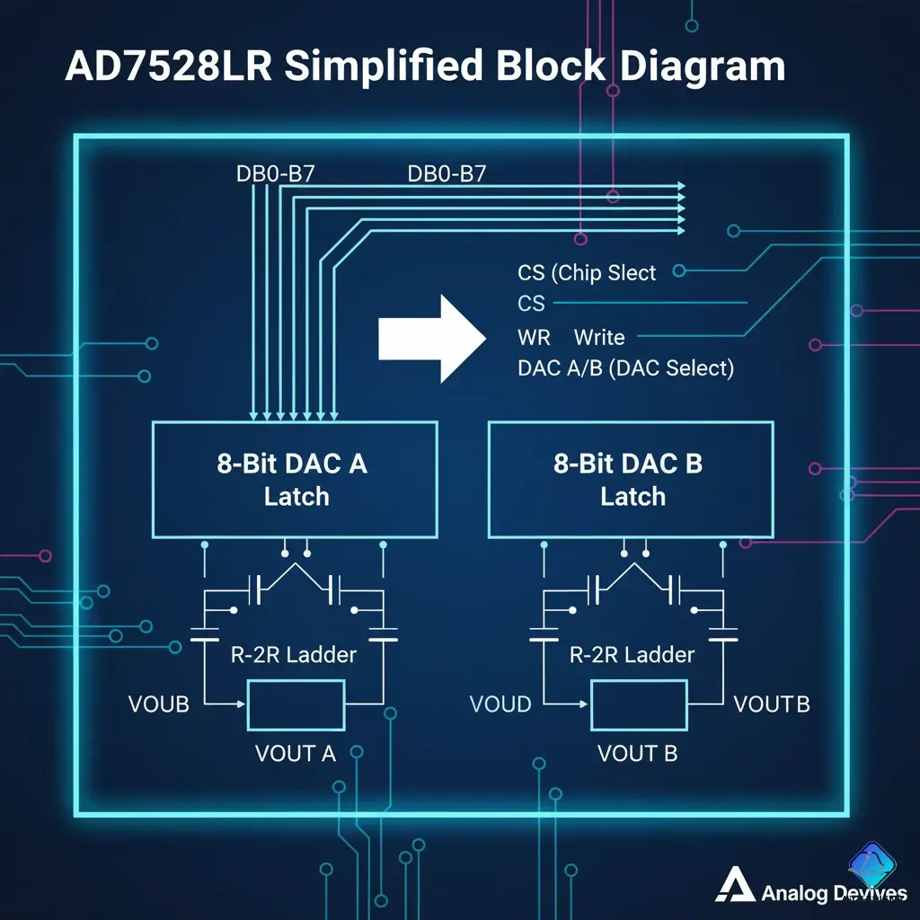
The AD7528LR is a monolithic dual 8-bit multiplying Digital-to-Analog Converter (DAC), originally manufactured by Analog Devices. It integrates two independent 8-bit DACs into a single 20-pin package, making it incredibly space-efficient for its time.
1.1 The Classic Dual 8-Bit CMOS DAC
This chip was revolutionary because it solved a common problem: how to get two separate, digitally-controlled analog outputs from a single shared 8-bit data bus. * **Dual DAC:** Contains two DACs (DAC A and DAC B). * **8-Bit:** Each DAC has 8 bits of resolution, meaning it can take a digital number from 0 to 255 and produce a corresponding analog output level. * **Multiplying (CMOS):** It's a "multiplying" DAC, meaning its output voltage is the product of the digital input *and* an analog reference voltage. This allows you to use it as a digital attenuator or programmable-gain amplifier. * **Shared Bus:** Both DACs are loaded from the same 8-bit data pins (DB0-DB7), using a simple chip-select and address pin to choose which DAC gets the data.1.2 Decoding the "LR" Suffix
In the world of components, suffixes are everything. For the AD7528: * **L:** Indicates a specific grade of linearity. * **R:** Refers to the package type, a 20-Lead SOIC (Small-Outline Integrated Circuit). You will also see this part as the **AD7528KN** (PDIP) or **AD7528JP** (PLCC). The **AD7528LR** is the surface-mount SOIC version.1.3 Key Specifications from the Datasheet
When you're trying to validate or replace this part, these are the specs that matter.| Parameter | Value | What it Means |
|---|---|---|
| Device Family | AD7528 | A classic CMOS multiplying DAC. |
| Resolution | 8 Bits | 256 possible output steps. |
| Number of DACs | 2 | Two independent DACs in one chip. |
| Interface | 8-Bit Parallel | Designed for classic microprocessor data buses. |
| Supply Voltage (VDD) | +5V to +15V | Highly flexible, works with 5V or 12V/15V systems. |
| Settling Time | 80 ns (typ) | Very fast. The analog output updates quickly after data is written. |
| Linearity Error | ±1 LSB (max) | Guarantees no missing codes and monotonic behavior. |
| Package | 20-Lead SOIC | The "LR" or "RS" suffix. |
2.0 AD7528LR Pinout (SOIC-20 & PDIP-20)
The AD7528LR pinout is identical for both the 20-pin SOIC and 20-pin PDIP packages, making it easy to identify on a board.
2.1 Pin Functions Explained (Data, Control, DAC I/O)
Understanding the pin functions is key to troubleshooting or interfacing with the chip.| Pin(s) | Name | Type | Function |
|---|---|---|---|
| 1 | VREFB | Analog Input | Reference Voltage for DAC B. |
| 2 | OUT B | Analog Output | Buffered Output of DAC B (requires external op-amp). |
| 3 | RFBB | Analog I/O | Feedback Resistor for DAC B's external op-amp. |
| 4 | AGND | Ground | Analog Ground. |
| 5 | VDD | Power | Positive Supply Voltage (+5V to +15V). |
| 6 | DGND | Ground | Digital Ground. |
| 7 | WR (Write) | Digital Input | Write Strobe. Latching data on the rising edge. |
| 8 | CS (Chip Select) | Digital Input | Chip Select (Active Low). Enables the write operation. |
| 9 | DAC A/B | Digital Input | DAC Select (0 = DAC A, 1 = DAC B). |
| 10-17 | DB0 - DB7 | Digital Input | 8-Bit Parallel Data Bus. |
| 18 | RFBA | Analog I/O | Feedback Resistor for DAC A's external op-amp. |
| 19 | OUT A | Analog Output | Buffered Output of DAC A (requires external op-amp). |
| 20 | VREFA | Analog Input | Reference Voltage for DAC A. |
Expert Tip: The AD7528LR is a CMOS multiplying DAC, which means its output is a current (IOUT). To get a voltage output, you must use an external operational amplifier as an I-to-V (current-to-voltage) converter. The on-chip RFBA and RFBB pins are provided as the feedback resistors for these op-amps to ensure perfect gain tracking.
3.0 AD7528LR Applications and Use Cases
This chip was designed for one thing: giving 8-bit microprocessors analog "hands." You'll find it in any legacy system that needed digitally-controlled analog signals.
3.1 Digital-to-Analog Conversion for Microprocessors
This is its primary job. A microprocessor (like an 8085 or Z80) would place a value on the data bus, select DAC A or B, and pulse the write line. The AD7528LR would "catch" that digital byte and convert it to a steady analog voltage.- Digital audio synthesis (e.g., in vintage samplers and drum machines).
- Automatic test equipment (ATE) to generate test voltages.
- CRT monitor and oscilloscope X-Y (vector) controls.
3.2 Digitally Controlled Gain/Attenuation
Because it's a "multiplying" DAC, you can use it as a digital potentiometer. * **Application:** Apply your analog audio signal to the VREF input. * **Control:** Write a digital value from 0 to 255 to the data bus. * **Result:** The output signal at VOUT will be a scaled (attenuated) version of your input signal. This is a classic method for creating a digitally controlled volume knob.3.3 Status as a Legacy Component
As of **2025**, the **IC AD7528LR** is a mature, **obsolete component**. It is **Not Recommended for New Designs (NRND)**. * Modern designs use DACs with serial interfaces like **I²C or SPI** to save pins. * Modern DACs offer much higher resolution (12-bit, 16-bit, or even 24-bit).However, its obsolescence makes it more valuable to the MRO (Maintenance, Repair, and Operations) market. A manufacturing line that runs on a 20-year-old controller can't be "upgraded" easily. Repairing the existing board with a genuine AD7528LR is the only viable option.
4.0 How to Use the AD7528LR: Interface & Design
Interfacing with the AD7528LR is a classic lesson in 8-bit parallel bus design.
4.1 Understanding the 8-Bit Microprocessor Interface
This chip is designed to look just like a memory location to your microprocessor. Here’s the write cycle: 1. The microprocessor places the 8-bit data value on the data bus (DB0-DB7). 2. The microprocessor's address decoding logic selects the chip by pulling **CS (Pin 8) low**. 3. The microprocessor's address bus sets **DAC A/B (Pin 9)** to 0 or 1 to select which DAC to update. 4. The microprocessor pulses the **WR (Pin 7) line low-to-high** to latch the data.This entire operation takes just a few nanoseconds and can be repeated thousands of times per second to generate waveforms.
4.2 Basic Unipolar Operation Circuit
This is the most common circuit. It shows how to connect an external op-amp to get a 0V to VREF output.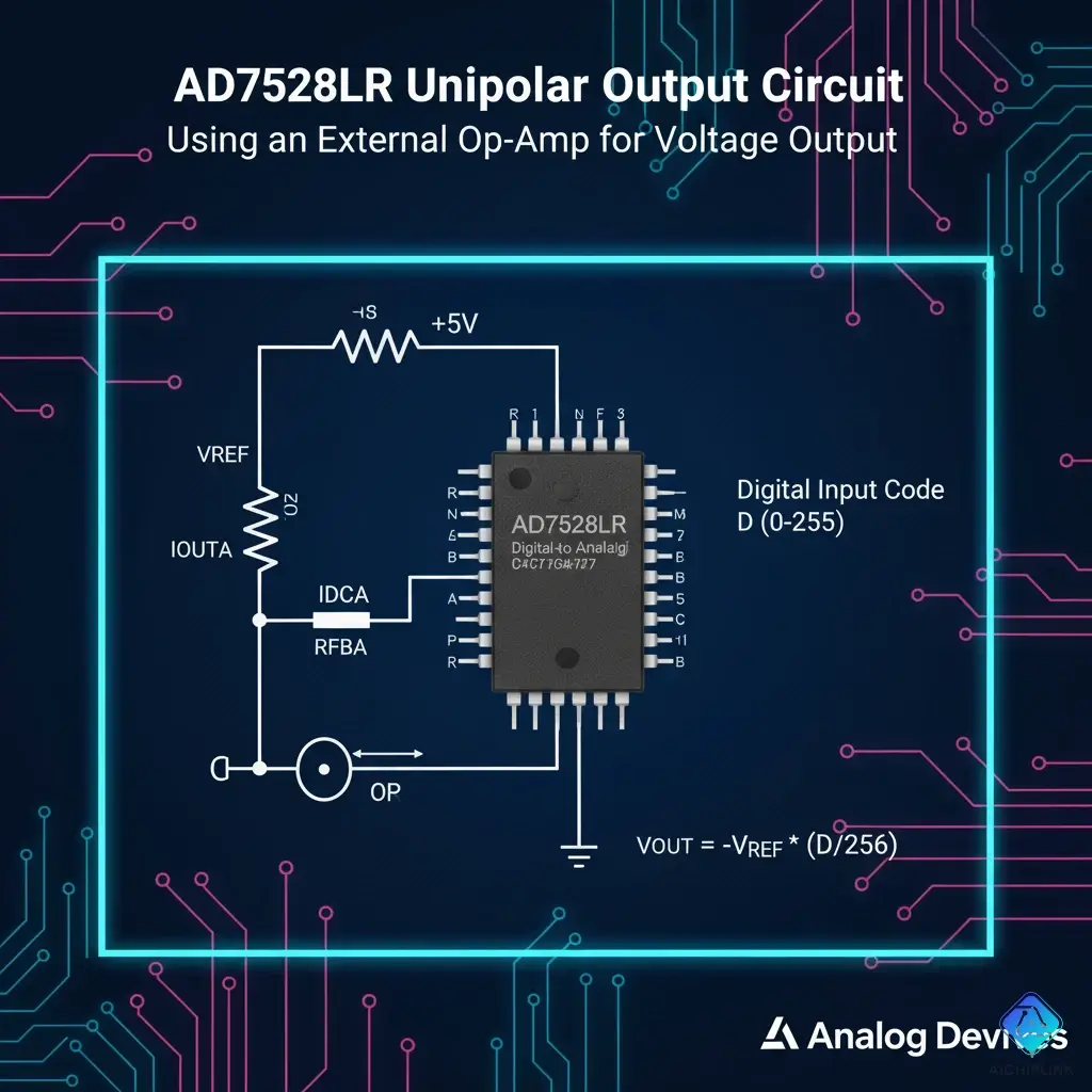
4.3 Finding an AD7528LR Equivalent or Replacement
As this is a legacy part, finding a "drop-in" replacement is difficult. * **Direct Replacement:** The best option is to source an original **AD7528LR** or another package variant like the **AD7528KN**. * **Pin-Compatible Equivalents:** Other manufacturers made similar parts, such as the **PM7528**. You **must** check the datasheet for pin compatibility and electrical characteristics. * **Modern Redesign:** For new designs, you would not use this part. You would select a modern dual 8-bit DAC with an I²C or SPI interface, such as a **MCP4728** or **DAC082S085**. These are not pin-compatible and require a full PCB redesign.Conclusion: A Critical Legacy Component
The IC AD7528LR is a perfect example of a foundational component that bridges the early digital and analog worlds. Its simple, parallel-bus interface and dual-channel output made it an incredibly versatile and popular chip for a generation of designers. While modern serial-interface DACs have replaced it in new designs, the AD7528LR remains an indispensable part for keeping critical, long-life systems in operation.
If you are an engineer or technician tasked with repairing a board that has an AD7528LR on it, you know that finding a reliable, genuine replacement is the most important step.
You need a partner who understands the challenges of sourcing mature and obsolete components. For all your legacy data converter needs, browse our full catalog of contact AichipLink today to secure the components required to keep your systems running.

Written by Jack Elliott from AIChipLink.
AIChipLink, one of the fastest-growing global independent electronic components distributors in the world, offers millions of products from thousands of manufacturers, and many of our in-stock parts is available to ship same day.
We mainly source and distribute integrated circuit (IC) products of brands such as Broadcom, Microchip, Texas Instruments, Infineon, NXP, Analog Devices, Qualcomm, Intel, etc., which are widely used in communication & network, telecom, industrial control, new energy and automotive electronics.
Empowered by AI, Linked to the Future. Get started on AIChipLink.com and submit your RFQ online today!
Frequently Asked Questions
What is the AD7528LR?
The AD7528LR is a classic monolithic dual 8-bit multiplying Digital-to-Analog Converter (DAC) from Analog Devices. It contains two independent 8-bit DACs in a single 20-pin SOIC package. It is designed to be interfaced directly with an 8-bit microprocessor bus.
What is the AD7528LR used for?
It is used in legacy systems to generate two independent, digitally-controlled analog voltage or current outputs. Its most common applications are in digitally controlled gain/attenuation (like a digital volume knob), audio synthesis, and automatic test equipment.
Is the AD7528LR obsolete?
Yes, the AD7528LR is a mature, legacy component and is considered obsolete or 'Not Recommended for New Designs' (NRND). It is primarily sourced for the maintenance, repair, and replacement (MRO) of existing equipment that was designed in the 1980s and 1990s.
What is the difference between the AD7528LR and AD7528KN?
The core silicon chip is the same. The difference is the package. The AD7528LR(or AD7528J**R**) is a 20-pin SOIC (surface-mount) package. The AD7528KN is a 20-pin PDIP (through-hole) package. They are functionally identical but not physically interchangeable without a new PCB layout.
Why does the AD7528LR need an external op-amp?
The AD7528LR is a multiplying DAC with a current output (I<sub>OUT</sub>). This raw output is not a stable voltage. An external op-amp is required to act as a current-to-voltage (I-to-V) converter, turning the DAC's output current into a stable, usable output voltage. The chip includes on-board feedback resistors (R<sub>FB</sub>) to ensure this conversion is accurate.


