Electronic design automation, or EDA, uses special tools to help engineers build hard electronic systems. EDA software and services help with planning, testing, checking, and making the products. These tools are very important for making today’s electronics stronger and better.
The worldwide EDA software market was $15.85 billion in 2024. Experts think it will keep growing as people want faster and smarter devices.
| Year | Market Size (USD Billion) |
|---|---|
| 2024 | 15.85 |
Companies use design automation to handle more difficult chips and circuits. EDA lets engineers work quicker, make better products, and follow new industry changes.
Key Takeaways
- Electronic Design Automation (EDA) uses special software. This software helps engineers design and test electronic systems faster. It also helps them make fewer mistakes. EDA tools do hard jobs like circuit design, simulation, verification, and layout. These tools make it easier to build good and advanced electronics. Using EDA saves time and money. It finds problems early and makes work more accurate. It also helps teams work well together. New trends like artificial intelligence and cloud computing are making EDA tools smarter. These trends make EDA tools more powerful. They help speed up design and testing. EDA is very important in many industries. It helps create new things in devices like smartphones, cars, medical equipment, and IoT gadgets.
Electronic Design Automation Overview
What Is EDA?
Electronic design automation, or EDA, helps engineers make hard electronic systems. EDA software lets computers do the work instead of people. These systems use computers to design, model, and test circuits. Engineers use EDA for printed circuit boards, integrated circuits, and microprocessors. EDA software checks for mistakes before making the product. This step makes sure products work well and do not break.
EDA systems have many special tools and platforms.
-
PCB design tools help engineers plan and draw circuit boards.
-
IC packaging design and analysis tools help put chips together and keep them safe.
-
Signal and power integrity analysis tools look for problems in signals.
-
RF and microwave design tools help with wireless systems.
-
Computational fluid dynamics and thermal analysis tools control heat and air in devices.
-
Molecular simulation tools help with new materials.
-
Cloud-based solutions let engineers work together from anywhere.
EDA tools now use artificial intelligence to make design faster and more correct. Shift-left methods help engineers find problems sooner. Some popular platforms are Allegro X Design Platform, Sigrity X Platform, and AWR Design Environment. These platforms help engineers with every step, from idea to making the product.
New EDA tools have changed how semiconductors are made. Engineers use FinFET and GAAFET technology to make smaller and stronger chips. EDA tools use AI to make chips better and use less power. Multi-die packaging lets engineers make more complex IC designs. Emulation platforms and FPGA prototyping help test designs before making them. More people want EDA in cars, planes, defense, and electronics for everyday use.
EDA helps manage silicon chips by checking and improving them from start to finish.
EDA vs. General CAD
EDA tools are not the same as general computer-aided design software. General CAD software is for mechanical or building design. EDA software is only for electronic systems. EDA tools have special features for electronic design.
| Feature | EDA Tools | General CAD Software |
|---|---|---|
| Logic Synthesis | Yes | No |
| Behavioral Synthesis | Yes | No |
| Intelligent Verification | Yes | No |
| Physical Verification | Yes | No |
| Timing Analysis | Yes | No |
| Hardware Emulation | Yes | No |
| Rapid Prototyping | Yes | No |
| IC, PCB, IoT Design | Yes | No |
| Mechanical Design | No | Yes |
| Architectural Design | No | Yes |
EDA tools use logic synthesis to turn how circuits act into logic gates. Behavioral synthesis changes high-level ideas into circuit designs. Intelligent verification finds mistakes fast. Physical verification checks if the design follows the rules. Timing analysis makes sure circuits work at the right speed. These features help engineers with hard IC and PCB designs.
EDA software also helps with hardware emulation and rapid prototyping. These features let engineers test and check designs before making them. EDA tools help with semiconductor intellectual property management and make sure designs follow the rules. Technology computer-aided design helps engineers test and improve semiconductor devices.
EDA software is important in many industries. Engineers use EDA for IC design, PCB design, IoT devices, car electronics, communication systems, and medical devices. EDA tools help companies make strong and new products.
Why EDA Matters
Managing Complexity
Modern electronic systems are much harder to design now. Engineers have many problems when making new products. EDA helps them handle these hard tasks and build devices that work well. Some common problems are:
-
Signal integrity problems, like crosstalk, jitter, and reflections.
-
Power integrity issues, such as voltage drops and noise.
-
Electromagnetic interference (EMI) and electromagnetic compatibility (EMC) worries.
-
Timing and synchronization, like clock distribution and timing budgets.
-
Following strict rules, such as Ethernet, DDR5, and PCIe.
-
Thermal management to control heat in small ICs and PCBs.
-
Hard semiconductor design, including SoCs and chiplets.
-
Multi-layer PCB design and layout checks.
-
Incomplete datasheets that need extra simulation.
-
Tool integration, time pressure, and more complex products.
EDA tools help by giving early simulation, analysis, and design checks. They help engineers stop expensive mistakes and finish faster. EDA lets engineers use different design levels, from big ideas to real layouts. This makes it easier to work on large IC and PCB projects. Teams can break big systems into smaller parts using hierarchical and modular design. EDA also lets engineers test and build models with simulation and emulation. This makes devices more reliable and easier to grow.
Improving Accuracy
Accuracy is very important in circuit and semiconductor design. EDA tools have changed how engineers check their work and make sure products work right. Some big improvements are:
-
Early simulation tools, like SPICE, let engineers test designs before building.
-
Logic synthesis tools help designers use higher-level models and make fewer mistakes.
-
Automated layout checks, like Optical Proximity Correction, help small IC features be more accurate.
-
Design for Testability (DFT) and Automatic Test Pattern Generation (ATPG) tools find faults and make products more reliable.
-
Integrated workflows for modeling, simulation, and checking catch mistakes early and save time.
EDA tools also have automatic features that make work easier. These features cut down on boring tasks and let engineers be creative. With better accuracy, companies can make high-quality ICs and PCBs that follow strict rules. EDA helps teams work on bigger projects without losing quality. Because of this, EDA is now very important for making advanced electronic systems.
EDA Tools

Electronic design automation tools help engineers at every step. These tools guide the whole process, from idea to finished product. EDA tools help with design entry, simulation, checking, and layout. Each tool has a special job in pcb design and ic development.
Design Entry
Design entry tools help engineers begin their projects. Old EDA tools changed hand-drawn plans into digital ones. This made it easier to make complex ic and pcb designs. Today, design tools link electrical plans with physical layouts. When engineers add a part to a plan, the layout updates by itself. This keeps everything matched and lowers mistakes. The user interface is smart and simple to use. It helps engineers work faster. Custom design flows fit modern pcb and ic projects.
Design entry tools help capture ideas and turn them into real designs.
Simulation
Simulation tools let engineers test circuits before building them. These tools show how circuits act and help find problems early. Simulation means fewer real prototypes and saves time and money. Engineers use simulation to check how things work and improve designs. It helps avoid expensive errors. Popular simulation platforms are Proteus, Autodesk Eagle, LTspice, and PSIM. These tools work for both pcb and ic projects.
| Software | Key Features & Use Cases |
|---|---|
| Proteus | Circuit simulation, pcb design, microcontroller support |
| Autodesk Eagle | Schematic and pcb editor, simulation, multi-layer support |
| LTspice | SPICE simulation, schematic capture, waveform viewer |
| PSIM | Power electronics and motor drive simulation |
Verification
Verification tools check if designs follow all rules and work right. These tools run after the design is made. They include simulation, rule checking, layout checks, and timing analysis. Verification tools help engineers find and fix mistakes before making the product. This step stops costly errors and makes products more reliable. In digital systems, verification uses metric-driven methods and Universal Verification Methodology. Analog systems focus on performance checks and simulations. Mixed-signal tools use both ways for hard ic and pcb designs.
Layout
Layout tools turn plans into real designs. They handle where parts go, routing, and multi-layer pcb design. Layout tools help with autorouting and high-speed digital design. These are important for signal integrity. The layout process includes checks like Design Rule Checks and Layout Versus Schematic analysis. These features help stop mistakes and make sure the design can be built. Automation and optimization in layout tools save time and make products better. AI and machine learning now help with faster prototyping and finding defects.
EDA tools link design and checking with manufacturing. They automate jobs like making the Bill of Materials and checking designs. This makes production faster, lowers mistakes, and cuts costs. EDA tools help move from idea to finished pcb or ic quickly and correctly.
Benefits of Design Automation
Efficiency
Design automation makes building electronic systems much faster. Engineers use smart tools to finish their work quickly. Some EDA tools use large language models to speed up tasks. For example, one tool can make design steps 25 times faster. The table below shows how different tools help with speed:
| Approach | Quantitative Metric | Description |
|---|---|---|
| LCDA | 25x speedup | Shows a 25 times faster way to finish design tasks. |
| Chip-Chat | End-to-end design capability | Can reach RTL-level plans with little help from people, but does not give a speed number. |
| GPT4AIGChip | Quantitative performance metrics | Balances speed and quality, with better results if the demo is good. |
Design automation lets teams work on bigger projects. Computers can handle harder designs without slowing down. This means companies can make new products faster.
Cost Savings
Design automation helps companies spend less money. Early simulation and testing tools find problems before anything is built. Fixing mistakes early is much cheaper than fixing them later. Following rules like UL certification lowers the chance of costly mistakes. Teams also save money by reusing old designs and working together better.
-
Simulation and checking tools find errors before building, so mistakes cost less.
-
Using old designs and breaking projects into parts saves time and makes things the same.
-
Working together with special tools helps teams finish faster.
-
Making sure designs are easy to build helps spot problems early and makes more good products.
-
Letting experts do hard jobs can lower costs.
These benefits help companies keep costs low and stay ahead of others.
Quality
Quality gets better when engineers use design automation. EDA tools make sure high standards are used from the start. This stops mistakes from spreading. These tools use numbers like test coverage, defect density, and test stability to check quality. The chart below shows some main ways to measure better quality:
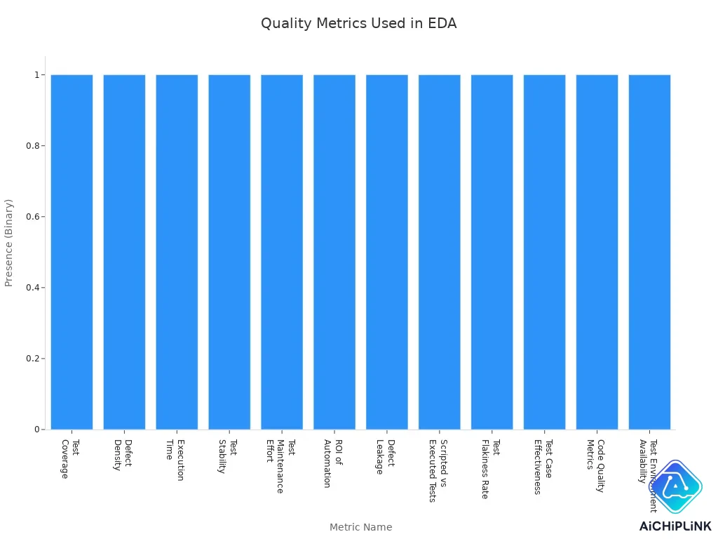
Engineers can see how many tests pass, how many mistakes show up, and if tests stay steady over time. These checks help teams keep their designs safe and strong. Design automation also helps teams keep quality high as projects get bigger. By using these tools, companies can give better products to customers.
Trends in EDA
AI Integration
AI is changing how engineers make chips and circuits. It helps with many steps in design. AI can do jobs like drawing plans, placing parts, and connecting wires. This makes work faster and helps stop mistakes. Machine learning finds problems early, like signal issues or wasted power. AI tests many designs quickly to pick the best one. It can adjust settings for better speed, less power use, and lower cost.
Engineers use AI to make layout, logic synthesis, and checking faster. This matters for new chips in AI and 5G devices. AI helps testing by finding rare problems and making sure designs work well. In printed circuit board design, AI helps with layout, routing, and heat control. It can spot possible defects before making the product. These changes help manage chips from design to end of life.
Companies such as Cadence, Synopsys, and Siemens are leaders in using AI in EDA tools. They help engineers handle hard designs and keep up with new technology.
Cloud Solutions
Cloud solutions are changing EDA by giving flexible resources. Engineers can run big tests and checks without needing costly computers. Cloud EDA lets teams from all over work together at the same time. This makes projects faster and helps companies launch products sooner.
-
Cloud EDA gives strong computing and safe data storage.
-
Teams can rent more computing power when needed, saving money and time.
-
Cloud systems help manage chips by tracking data and updates.
Cloud use also makes security better. Providers use strong encryption and multi-factor authentication to keep designs safe. Hybrid cloud mixes public and private clouds for more control and following rules. Groups like IEEE CEDA help by sharing knowledge and setting standards. Global teamwork grows as cloud EDA connects teams in North America, Asia-Pacific, and Europe. This teamwork helps solve hard problems and brings new ideas to the industry.
The EDA market keeps growing as more companies use cloud and AI to handle bigger and harder designs.
Electronic design automation helps make electronics better and faster. It makes designing easier, smarter, and more correct. The world market is getting bigger because of new things like 5G and self-driving cars.
-
EDA tools let engineers make new chips, IoT gadgets, and car electronics.
-
AI and cloud tools help teams work together and make better designs.
-
Companies use EDA to save time, fix fewer errors, and build good products.
| Aspect | Impact on Electronics Industry |
|---|---|
| Innovation Support | AI and automation make design quicker and more right |
| Career Opportunities | More jobs for people who know AI, cloud, and chip design |
| Regional Growth | Asia-Pacific grows fast with big spending and new work |
Students and workers can find jobs in electronics by learning about design automation. This field has many ways to grow and try new ideas.
FAQ
What is the main goal of electronic design automation?
The main goal of electronic design automation is to help engineers build hard electronic systems. These systems can be chips or circuit boards. The tools make work faster and help engineers avoid mistakes.
How do EDA tools improve efficiency in circuit design?
EDA tools let engineers try out and check circuits before making them. This saves time and helps stop errors. Teams can finish their work faster and use less effort.
Why is design verification important in the PCB design process?
Design verification checks if a PCB follows all the rules and works right. This step finds mistakes early. It helps stop big problems when making the product.
What role does optimization play in semiconductor design?
Optimization helps engineers make chips that work better. It makes them faster, use less power, and be smaller. Engineers use special ways to get the best chip.
How does scalability affect silicon lifecycle management?
Scalability lets engineers work on bigger and harder projects. Silicon lifecycle management keeps track of chips from start to finish. This helps companies handle products as they get bigger.

Written by Jack Elliott from AIChipLink.
AIChipLink, one of the fastest-growing global independent electronic components distributors in the world, offers millions of products from thousands of manufacturers, and many of our in-stock parts is available to ship same day.
We mainly source and distribute integrated circuit (IC) products of brands such as Broadcom, Microchip, Texas Instruments, Infineon, NXP, Analog Devices, Qualcomm, Intel, etc., which are widely used in communication & network, telecom, industrial control, new energy and automotive electronics.
Empowered by AI, Linked to the Future. Get started on AIChipLink.com and submit your RFQ online today!