LM723 Voltage Regulator Circuit: A Complete Guide to Pinout and Specifications
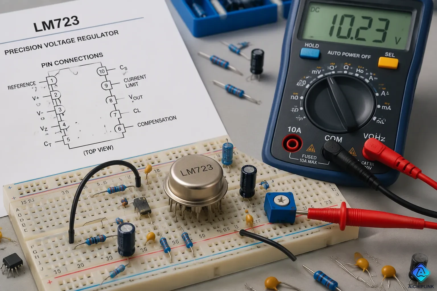
The LM723 is a classic adjustable linear voltage regulator IC. Engineers mainly build it for series regulator applications. This single-chip programmable voltage regulator offers a wide output voltage range and adjustable current limiting. It delivers 150 mA without an external pass transistor. The device also supports regulation below 7V.
Hobbyists and professionals value the chip for its flexibility. A clear grasp of the pinout and specifications makes the lm723 voltage regulator circuit easier to design and troubleshoot. Careful study pays off in stable, current-limited supplies. The part remains a favorite teaching tool. Its simple external network keeps builds approachable. Many bench supplies still use it.
Key Takeaways
-
The LM723 is a classic adjustable voltage regulator IC. It gives a steady output voltage from 2V to 37V.
-
The LM723 has 14 pins. Each pin does a certain job, like input, output, reference, and current limit.
-
You can set the output voltage using two resistors. The formula is Vout = 7.15V × (R1 + R2) / R2.
-
The LM723 limits current with a sense resistor. The limit trips at about 0.6V across the resistor.
-
The LM723 is helpful for learning and for older designs. Newer regulators give better performance for new projects.
Inside the LM723 Voltage Regulator Circuit
Key Features and Capabilities
The LM723 is a single-chip programmable voltage regulator. Designers mainly use it for series regulator applications. The chip packs a voltage reference, an error amplifier, a series pass transistor, and current limiting circuitry all on one die. This internal setup makes the lm723 voltage regulator circuit flexible for many supply designs.
The device gives you an output voltage you can adjust from 2 to 37V using external resistors. It takes a maximum input voltage of 40V. The output current of 150mA without an external pass transistor works well for light loads. Adding an external pass transistor boosts the current capability up to 10A. A precise 7.15V reference sits on the Vref pin. Built-in protection covers foldback current limiting, short-circuit current limit, and thermal shutdown. Ripple rejection reaches about 74 dB, and output noise stays near 86 µV rms.
| Feature | Detail |
|---|---|
| Output voltage | 2 V to 37 V, set by external resistors |
| Maximum input voltage | 40 V |
| Output current, no pass transistor | 150 mA |
| Output current, with pass transistor | up to 10 A |
| Internal reference | 7.15 V |
| Protection | Foldback limiting, short-circuit limit, thermal shutdown |
Available Package Types
The LM723 comes in two main packages. The PDIP is a 14-pin through-hole plastic package. Hobbyists like it for breadboard work and prototyping. The TO-100 metal can serves needs for a wider temperature range. The UA723 equivalent adds 14PDIP, 14SO, and SOIC options, and the LM723CN plastic DIP variant works well for consumer builds.
Package choice affects how the pins map to a board layout. Through-hole parts fit sockets and hand assembly. Surface-mount variants save space on dense boards. Engineers should check the pin arrangement for their chosen package before routing a design. The electrical specifications stay mostly the same across packages.
LM723 Pinout
Pin Functions and Descriptions
The LM723 has a 14-pin layout, and every pin does a clear job. Pin 12 hooks up to the positive input supply terminal. Pin 7 hooks up to the negative terminal and acts as ground. Pin 6 gives the internal reference voltage of almost 7V. Pin 1 is not connected (NC), so no signal goes through it. Pin 2 works as the current limit terminal. Pin 3 serves as the current sense terminal for current limiting and foldback uses.
The other pins finish the control loop. Pin 4 is the inverting input, and it helps keep the output voltage steady. Pin 5 is the non-inverting input, and it gets the reference voltage for the internal op-amp. Pin 10 sends out the regulated output. Pin 11 feeds the collector of the series pass transistor, and designers tie it to the positive supply when they use no external transistor. Pin 9 helps with negative voltage regulator designs. Pin 13 takes a 100pF capacitor to cut down noise. Pins 8 and 14 are not connected either.
| Pin No. | Pin Name | Description |
|---|---|---|
| 1, 8, 14 | NC | Not connected |
| 2 | Current Limit | Sets maximum load current |
| 3 | Current Sense | Works with pin 2 for foldback limiting |
| 4 | Inverting input | Connects to the output divider |
| 5 | Non-inverting input | Tied to the internal reference |
| 6 | Vref | Reference voltage of nearly 7V |
| 7 | -Vcc | Ground |
| 9 | Vz | Used in negative regulator designs |
| 10 | Vout | Regulated output |
| 11 | Vc | Collector of the pass transistor |
| 12 | V+ | Positive supply input |
| 13 | Frequency Compensation | 100pF capacitor to ground |
Package and Pin Configuration Differences
The PDIP-14 package puts all 14 pins in two rows for through-hole assembly. The TO-100 metal can uses a round setup with fewer leads you can reach. This gap shapes the pinout setup on a board. A designer who moves a circuit between packages must remap every connection. The pin functions stay the same, but the physical order changes.
The UA723 family adds 14-pin DIP and SO-14 surface-mount choices. Package choice affects how heat is handled. Higher currents need an external pass transistor and a heat sink. The current limit point also shifts with temperature, because the sense transistor triggers at about 0.6V VBE and that value moves roughly -2 mV/°C. Engineers should check the ic pinout drawing for their exact package before routing traces. A careful review of the pinout stops wiring errors and protects the regulator during first power-up.
Internal Architecture
Voltage Reference and Error Amplifier
The LM723 divides its silicon into two working parts. A voltage reference section makes a steady 7.15V reference using a zener diode structure, not a bandgap. That reference can supply up to 15 mA, and its line and load regulation stay under 1 mV from 1 to 15 mA. Zener behavior means the reference shifts with temperature, so the voltage reference specifications matter most in precision designs. The regulator section holds the internal error amplifier, the pass device, and the limiting circuitry.
| Section | Function | Key Detail |
|---|---|---|
| Voltage reference | Zener-based stable reference | 7.15V nominal, 15 mA max, under 1 mV regulation over 1–15 mA |
| Regulator and control | Error amplifier compares reference against feedback | Works above and below 7.15V, 37V max input, 150 mA internal output |
The internal error amplifier closes the control loop. A feedback divider takes a sample of the output voltage and sends it to one amplifier input. The amplifier compares that feedback against the reference and adjusts the pass device drive. The same relation sets the output in both modes: output voltage = VREF × (R1 + R2) / R2. Below-reference mode (output under 7.15V) sends the divider tap to the amplifier input. Above-reference mode ties VREF to ground and connects the tap a different way. Either way, the loop fixes any error and keeps the voltage regulator output steady.
Series Pass Transistor and Current Limiting
Current limiting depends on a low-value sense resistor placed between the pass transistor emitter and ground. A dedicated sense transistor watches the drop across that resistor. When the drop goes past about 0.6V, equal to one base-emitter drop, the sense transistor turns on. It then pulls drive away from the pass transistor base, and the output current stops rising. Designers usually set the limit at 1.2 to 1.5 times the maximum load current and pick the resistor size from that target.
This threshold shifts with temperature at about -2 mV/°C, because it depends on the sense transistor's VBE. Precision builds need compensation or digital monitoring. The pass device itself works as an emitter follower, and external transistors extend the voltage regulator beyond the internal 150 mA.
LM723 Specifications
Absolute Maximum Ratings
Engineers must follow the absolute maximum ratings before they power any circuit. These limits mark the safe operating boundary for the device. The table below lists the key absolute maximum ratings for the LM723.
| Parameter | Absolute Maximum Rating | Notes |
|---|---|---|
| Reference section output current | 15 mA | Absolute maximum rating |
| Input voltage | 37 V | Absolute maximum rating |
| Internal output current | 150 mA | Without external pass transistor |
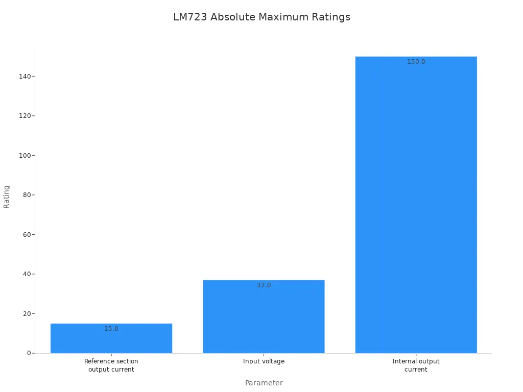
The reference section output current stops at 15 mA. The input voltage tops out at 37 V as an absolute maximum rating. The internal output current stays at 150 mA without an external pass transistor. Designers who go past these limits risk damage to the chip. The operating junction temperature range also limits safe use in hot environments.
Key Technical Specifications
The technical specifications show how the part acts in normal operation. The reference voltage is 7.15V nominal, and you get it at pin 6. The minimum input voltage is about 9V, which adds the 7V reference and roughly 3V dropout. The maximum output current reaches about 150 mA from the internal pass transistor. The current limit threshold is about 0.6V across the sense resistor, which equals the VBE of the sense transistor.
| Specification | Value / Detail |
|---|---|
| Reference voltage | ~7V (7.15V nominal) |
| Minimum input voltage | ~9V (7V reference + ~3V dropout) |
| Maximum output current (internal) | ~150 mA without external pass transistor |
| Current limit threshold | ~0.6V across sense resistor (VBE of sense transistor) |
| Current limit temperature coefficient | ~-2 mV/°C |
| Output voltage setting | Two-resistor divider |
| Reference type | Zener-based |
| Temperature stability | ~10x worse than typical bandgap references |
The voltage reference specifications show a zener-based design. This design has a temperature coefficient about 10x worse than typical bandgap references. The current limit threshold changes inversely with temperature at about -2 mV/°C. These electrical characteristics matter for precision builds. The output voltage setting uses a two-resistor divider. Designers connect the divider tap to the error amp input for outputs below 7.15V. For outputs above 7.15V, they tie VREF to ground and connect the tap a different way. The voltage - input and voltage - output ranges stay within the limits noted above. The current - output figure of 150 mA works for light loads. An external pass transistor pushes the maximum output current well past that figure. The maximum input voltage stays at 37V for safe operation. The input voltage up to 40v figure shows up in some datasheet variants, so engineers should check their exact part. The pins and their functions stay the same across packages. A careful review of these technical specifications leads to a reliable design.
Circuit Design Guide
Output Voltage and Current Calculations
A designer begins with the pinout and then moves outward to the external parts. The schematic diagram follows a simple pattern. The positive rail feeds pin 12, and ground returns to pin 7. The reference appears at pin 6, and the output leaves pin 10. The feedback divider connects to the error amplifier input. The current sense resistor sits between the pass transistor emitter and ground, and its ends reach pins 2 and 3.
Two formulas drive the whole design. The output voltage follows the divider ratio: output voltage = VREF × (R1 + R2) / R2, with VREF near 7.15V. The current limit follows the sense resistor: the limit trips when the drop across RS reaches about 0.6V, the base-emitter voltage of the sense transistor. A designer picks RS from the target load current. This threshold drifts at roughly −2 mV/°C, so precision builds need compensation.
| Calculation | Governing Principle | Formula / Threshold | Key Notes |
|---|---|---|---|
| Output voltage, below-reference mode | Divider samples the output and feeds the error amplifier | VOUT = VREF × (R1 + R2) / R2 | VREF ≈ 7.15V |
| Output voltage, above-reference mode | Divider tap compared against VREF | VOUT = VREF × (R1 + R2) / R2 | Same formula, different tap connection |
| Current limiting | Sense resistor detects the drop | Limit at VRS ≈ 0.6V | Sense transistor cuts pass drive |
| Current-limit drift | Threshold follows VBE | ≈ −2 mV/°C | Compensation needed for precision |
Practical Design Example
Think about a +12 V supply with a 50 mA current limit. The builder chooses R2 = 10 kΩ. Then R1 = (12/7.15) × 10k − 10k ≈ 6.78 kΩ. The sense resistor becomes Rsc = 0.65 V / 50 mA = 13 Ω. A third resistor, R3 = R1 parallel R2 ≈ 4.04 kΩ, minimizes temperature drift.
A second example shows the below-7V mode. The goal is a supply you can adjust from 2 V to 5 V with a 1.0 A limit. An external pass transistor carries the 1 A load, well past the internal 150 mA. The designer replaces R1 with a series potentiometer and resistor, selects a 10 kΩ pot, and derives the other resistors from the minimum and maximum output conditions. This programmable voltage regulator keeps the same pins and the same divider relation. The maximum output current now depends on the external transistor, not the chip alone. A careful review of the specifications before wiring saves rework later.
Typical Applications
Power Supply and Bench Supply Designs
Bench supplies are where the LM723 shows up most often. One popular design gives 30 V at 3 A without a fan. It has full voltage and current limiting, a floating ground, and real V/I metering on the output. The builder starts with a 230 VAC to 30 VAC transformer and a diode bridge made from doubled 1N5408 diodes. A 4700 µF filter capacitor and optional TVS protection complete the parts list.
The headroom check matters here. A 30 VAC secondary gives about 49 V peak, and two diode drops leave roughly 47 VDC. That is more than the 40 V limit of the voltage regulator. So the builder removes about 35 turns from the secondary to land near 40 VDC. A 1 A fuse covers a mains draw of 0.5 A or less and handles startup inrush. External 2N3055 pass transistors carry the load current.
Designers can also split the job into modules: a pre-regulator, a voltage regulator stage, a current regulator stage, and an output stage. Each module gets bench-tested alone. Failures stay local and easy to fix, but you need more parts and board space. A single-chip build saves space, but the loops share one error amplifier, so stability needs careful checking.
Battery Charging and Current-Limited Circuits
The LM723 supports adjustable current limiting through discrete sensing resistors. The resistor value follows Rsc = 0.66 / Maximum Current, with the sense voltage taken across the resistor. One practical bench supply drives an external emitter-follower transistor. It offers three switchable ranges near 15 mA, 150 mA, and 1.5 A. A millivolt meter across the sense resistor shows load current.
A foldback current limiting circuit adds real protection. The allowed current falls as the output voltage drops. It reaches a short-circuit value well below the normal maximum output current. This cuts pass-transistor dissipation during faults. Battery charging gets the same benefit from this control.
In battery charging applications, the LM723CN ensures precise control over the charging voltage and current, optimizing battery performance and longevity.
Strengths and Alternatives
Strengths and Limitations of the LM723
People stay loyal to the LM723 because it is cheap and tough. It is hard to beat for the price you pay. Other chips like the SG3532 and LAS1000 had better specs, but companies stopped making them. The 723 was just good enough and cost less. That is why it has stayed in catalogs and classrooms for so long.
The part also gives designers real freedom. When wired the right way, it makes a low-noise output. It takes an input up to about 40V and can drive external pass transistors. Designers can change its frequency response directly. The chip also works as a temperature controller, a negative regulator, a floating regulator, or a shunt regulator.
Its weak points need just as much attention. The LM723CN has no built-in thermal protection, so heat sinks and extra circuits must handle the heat. Current limiting can be adjusted, but it is not precise. The error amplifier gain is moderate, and its bias current is low. The lowest regulated output is near 2.5V, and the dropout voltage is about 10V. Overload conditions can also affect how sensitive the current limiting is. The device rewards careful handling, and beginners often find it hard to understand.
Comparison with Modern Regulator ICs
Modern regulator ICs differ from the LM723 in their main reference. The 723 uses a zener-based reference. Modern parts use bandgap references with much better temperature stability. A modern low-dropout regulator can also run from about 1.5V to 2V, while the 723 needs about 9V at its input. So the 723 is not recommended for new designs.
Different alternatives fit different jobs. The LM338 handles 5A with a bandgap reference. The LT1083, LT1084, and LT1085 families offer low dropout with high current. A TL431 paired with a pass transistor gives precise regulation. Modern LDO ICs from Micrel, TI, and Analog Devices serve precision, low-voltage, and high-efficiency designs.
The LM723 comes from a time when zener-based references were the best available. Modern bandgap-based LDOs offer better temperature stability, lower minimum input voltages, and better efficiency, so the LM723 is not recommended for new designs—though its design remains useful to understand and helpful for legacy maintenance and education.
The LM723 still fits legacy maintenance, education, and simple current limiting. Each option has a place, and the right voltage regulator depends on the job at hand.
The LM723 is still a flexible, proven choice for series regulator applications. Its wide output range, adjustable current limiting, and 150 mA internal output keep it useful for many builds. Readers who study the pinout, specifications, and design steps gain confidence with the lm723 voltage regulator circuit. They can size the feedback divider and sense resistor using clear formulas.
Designers should use the design guide on real projects. The LM723 works well where adjustable, current-limited regulation matters. Modern alternatives serve low-voltage and high-efficiency needs. Even so, this voltage regulator holds lasting value for learning and practical work. Careful wiring and honest respect for its limits reward the builder with a stable supply. The classic voltage regulator earns its place in any workshop.

Written by Jack Elliott from AIChipLink.
AIChipLink, one of the fastest-growing global independent electronic components distributors in the world, offers millions of products from thousands of manufacturers, and many of our in-stock parts is available to ship same day.
We mainly source and distribute integrated circuit (IC) products of brands such as Broadcom, Microchip, Texas Instruments, Infineon, NXP, Analog Devices, Qualcomm, Intel, etc., which are widely used in communication & network, telecom, industrial control, new energy and automotive electronics.
Empowered by AI, Linked to the Future. Get started on AIChipLink and submit your RFQ online today!
Frequently Asked Questions
What input voltage does the LM723 need?
The chip needs about 9V at its input. That number comes from the 7.15V reference plus about 3V of dropout. Some datasheet versions list a 40V maximum, so check your exact part. The pinout stays the same across packages.
How much current can the LM723 deliver on its own?
The internal pass transistor supplies about 150 mA. Designers add an external pass transistor for heavier loads. That external device carries the current, and the lm723 voltage regulator circuit then reaches much higher output levels.
How do I set the current limit?
Place a sense resistor between the pass transistor emitter and ground. The limit trips when the drop across it reaches about 0.6V. Pick the resistor value from the target load current. This voltage regulator threshold drifts at roughly −2 mV/°C.
Why does the reference voltage shift with temperature?
The LM723 uses a zener-based reference. Its temperature stability is about 10x worse than typical bandgap references. Precision builds need compensation or calibration. Many designers accept the drift in educational and legacy work.
Can the output go below 7V?
Yes. The device supports a below-reference mode for outputs under 7.15V. The designer sends the divider tap to the error amplifier input instead of tying VREF to ground. The same divider formula still sets the output.