Wide Band Differential Amplifier Calculator
The Wideband Differential Amplifier Calculator computes bias voltages, current levels, voltage gain, and frequency response for wideband differential amplifier circuits. Enter the amplifier parameters to quickly analyze and design differential amplifiers with accurate performance predictions.
Wide-band Differential Amplifier Calculator
Equations
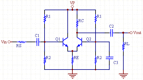
VB = VP*R2/(R1+R2)
VE = VB - VBE
IE = VE/RE
Alpha = Beta/(Beta+1);
IC = Alpha*IE
VC = VP - IC*RC/2
IB = IC/Beta
gm = Ic/25mA
re = Alpha/gm
rπ = Beta/gm
A = Alpha* rπ*RC/(Rs+2*rπ)/re
fP1 = 1/(2*π*(Rs||2*rπ)*(CBE/2+CBC))
fP2 = 1/(2*π*RC*CBC)
fT = gm/(2π*(CBE+CBC))
The lower pole is dominate.
Introduction
BJT: Differential Amplifier Explained
I. Wideband Differential Amplifier Calculator
This tool is designed to calculate critical performance metrics for wideband differential amplifiers, including current levels, bias voltage, gain, and frequency response.
What is a Wideband Amplifier?
A Wideband Differential Amplifier is an amplifier designed to maintain a precise amplification factor over a wide frequency range while providing high gain.
By using a specific configuration—tying the collector of the first transistor () to the base of the second () to signal ground—it is possible to overcome the Miller Capacitance limitations. The resulting gain-bandwidth product is orders of magnitude greater than that of standard common-emitter amplifiers.
II. Understanding Differential Amplifiers
2.1 What is a Differential Amplifier?
A Differential Amplifier (or difference amplifier) is a circuit that amplifies the difference between two input signals while rejecting any signals that are common to both inputs. It is the fundamental building block of the Operational Amplifier (Op-Amp).
The Formula: The basic output equation is:
Where:
- : Output Voltage
- : Differential Gain
- : Input Voltages
Ideally, if , the output is zero. The amplifier focuses purely on the gap between the two voltages.
2.2 Advantages
- Drift Elimination: They are excellent at minimizing "drift" (slow changes in voltage due to temperature fluctuations), making them ideal for precision instruments like oscilloscopes and voltmeters.
- Noise Rejection: They respond only to the difference signal and ignore Common-Mode Signals (noise or ground voltages present on both inputs).
2.3 Why are they used? (Noise Suppression)
Differential amplifiers are primarily used to suppress Noise.
- Common-Mode Noise: Electrical noise (from electromagnetic induction or ground loops) often affects both input wires equally.
- The Solution: Since the amplifier subtracts one input from the other (), any noise present on both lines is effectively cancelled out. This is vital in electrically noisy environments where weak signals can easily be corrupted.
2.4 Applications
- Medical Electronics: Amplifying weak bio-signals (like heart signals/ECG) for digital processing.
- Audio Systems: Used in volume control circuits and balanced audio lines.
- Modulation: Essential for amplitude modulation techniques.
- Automatic Gain Control (AGC): Used in control circuits requiring stable gain.
2.5 Configuration Types
- Dual Input, Balanced Output: Two inputs, differential output.
- Dual Input, Unbalanced Output: Two inputs, single-ended output.
- Single Input, Balanced Output: One input, differential output.
- Single Input, Unbalanced Output: One input, single-ended output.
III. Differential Amplifier Circuit Implementations
3.1 MOSFET Differential Amplifier
- Structure: Uses Metal-Oxide-Semiconductor Field-Effect Transistors (MOSFETs).
- Operation: The terminals (Sources) of both MOSFETs are connected to a constant current source.
- Behavior: If the input voltage exceeds the threshold, the MOSFET enters the active region (triode/saturation depending on load). The circuit relies on the balance between the two MOSFETs to steer current.
3.2 BJT Differential Amplifier
- Structure: Uses Bipolar Junction Transistors (BJTs). The Emitters of both transistors are tied together and connected to a common current source or ground resistor.
- Operation: Inputs are applied to the Bases; the output is typically taken from the Collectors.
- Mechanism: When an input is applied to Base 1 (), the voltage drop across the emitter resistor changes, altering the conduction of . Because the emitters are coupled, this change affects , allowing the circuit to amplify the difference signal.
3.3 Op-Amp Differential Amplifier
- Structure: Built using a standard Operational Amplifier with external resistors.
- Operation: Uses both the inverting (-) and non-inverting (+) terminals.
- Gain Control: Unlike raw transistor circuits, the gain here is easily determined by the ratio of external resistors.
- Note: For perfect differential operation, the ratio of the resistors on the inverting side must match the ratio on the non-inverting side.
Frequently Asked Questions
What does the Wide Band Differential Amplifier Calculator calculate?
The calculator determines critical parameters for designing wide-band differential amplifiers/ including current levels (IC/ IE/ IB)/ bias voltages (VB/ VE/ VC)/ voltage gain (A)/ and frequency response (fP1/ fP2). It also calculates transconductance (gm)/ input resistance (rπ)/ and other key metrics using user-provided resistor values/ supply voltage/ and transistor specifications.
How does this amplifier overcome Miller capacitance limitations?
The design ties the collector of Q1 and the base of Q2 to signal ground/ bypassing the Miller effect. This configuration significantly improves gain-bandwidth compared to common-emitter amplifiers/ enabling high-frequency performance without stability issues.
What parameters are required to use the calculator?
Inputs include resistor values (R1/ R2/ RC/ RE)/ supply voltage (VP)/ transistor Beta (β)/ base-emitter voltage (VBE)/ current gain-bandwidth product (fT)/ and parasitic capacitances (CBC/ optional CBE). Source resistance (Rs) and load resistance (RL) are also needed for accurate gain and frequency calculations.
How does Beta (β) influence the amplifier’s performance?
Beta affects DC current gain/ directly impacting collector current (IC = β*IB) and input resistance (rπ = β/gm). Higher Beta increases voltage gain and input impedance but requires careful thermal and stability management to avoid drift or distortion.
Why is the lower pole (fP1) dominant in the frequency response?
The lower pole fP1 dominates because it arises from the input stage’s RC network (Rs || 2rπ interacting with CBE/2 and CBC). This pole defines the amplifier’s -3dB bandwidth/ while fP2 (from the output RC network) typically lies at higher frequencies due to smaller RC time constants.
Hot SKU
Related Tools
Resistor Color Code Calculator
AIChipLink’s Resistor Color Code Calculator is an interactive tool for identifying resistor values based on 4-band, 5-band, and 6-band color codes. Simply select the colors, and the calculator will display the resistance in Ohms (Ω), tolerance, and power rating. Whether you are building a circuit, repairing electronics, or sorting resistors in your lab, this calculator provides an accurate and efficient way to decode resistor values.
Ohms Law Calculator
AIChipLink’s Ohm’s Law Calculator helps engineers and students quickly calculate resistance, current, voltage, and power in an electrical circuit. Simply enter any two known values, and the calculator will instantly compute the remaining parameters. This fast and easy-to-use online tool illustrates the fundamental relationship between voltage, current, and resistance, making it essential for circuit design, troubleshooting, and electronics learning.
Op-Amp Voltage and Gain Calculator
The Op Amp Voltage and Gain Calculator is an easy-to-use tool for analyzing operational amplifier circuits. It calculates the output voltage, inverting gain, and non-inverting gain based on the input parameters. Simply enter the values of V1, V2, Vp, Vn, and the resistor values R1, R2, R3, and R4, and the calculator will instantly provide accurate results. This tool is suitable for both professional engineers and beginners learning op amp circuit design.
Inverting Op-Amp Resistor Calculator
The Inverting Op Amp Resistor Calculator is a practical tool for analyzing operational amplifier inverting circuits. By entering parameters such as the desired gain, output voltage (Vout), R1 resistance, and the input voltages V1, V2, Vp, and Vn, the calculator automatically determines the required resistor values (R2, R3, and R4). Simply input the values and click “Calculate” to quickly design and verify inverting op amp configurations.
AIChipLink – Your Trusted Electronic Components Distributor
12.28 M
Listed Part Number3,000+
Leading Manufacturers4.9 M
In-stock SKU15,000+
Warehouse Area(㎡)


