BJT Cascode Amplifier Calculator
This BJT Cascode Amplifier Calculator computes bias voltages and currents, voltage gain, and frequency response for a Cascode amplifier. Simply enter the amplifier parameters and click “Compute” to instantly calculate bias levels, gain, and frequency characteristics, helping you analyze and design Cascode amplifier circuits efficiently.
BJT Cascode Amplifier Calculator
Equations
VB1 = R3/(R1+R2+R3)
VB2 = (R2+R3)/(R1+R2+R3)
VE1 = VB1 - VBE
VE2 = VB2 - VBE
VC1 = VE2
VC2 = VP - IC*RC
RB1 = R3*(R1+R2)/(R1+R2+R3)
IB*RB1 + IB*Beta*RE + VBE = VB1
IB = (VB1 - VBE)/(RB1 + Beta*RE)
IC = Beta*IB
gm = Ic/25mA
rπ = Beta/gm
If RE2 is zero ohms:
A = -gm*((RL||RC)*(R2||R3))/(R23+RS)*(rπ/(rπ+Rx+(R2||R3||RS))
else
A = -(RL||RC)/RE2
Rx is typically 10-30 ohms, we use 20 in the calculator.
fT = gm/(2π*(CBE+CBC))
f1 = 1/(Rin*(Cbe+2*Ccb))/(2*π)
f2 = 1/(RL*Ccb)/(2*π)
The lower pole is dominate:
BW = f1

Introduction
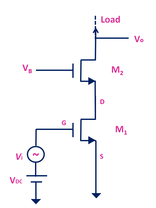
Cascode Amplifier (BJT): DC Analysis & Multistage Amplifiers
Introduction to the Cascode Amplifier Calculator
This BJT Amplifier online calculator is designed to compute bias voltages, currents, voltage gain, and frequency response for a Cascode amplifier configuration.
The Cascode amplifier is renowned for its high gain and exceptionally wide bandwidth. By utilizing a second transistor as a common-base current buffer, the initial common-emitter stage overcomes the limitations caused by the Miller Effect. Consequently, this configuration allows for gain-bandwidth products orders of magnitude larger than a standard common-emitter amplifier.
Key Design Considerations:
- Voltage Supply: Since two transistors are stacked vertically, a higher voltage supply is often required to maintain decent operating margins for both devices.
- Gain Control: The gain is roughly determined by the ratio .
- Bandwidth: A higher sum of emitter resistances () generally contributes to greater bandwidth stability.
- Buffering: For real-world applications above 2 MHz, an output buffer (like an emitter follower) is recommended to prevent loading effects. Measuring high-frequency response directly with a standard 1 MHz scope probe without a buffer will artificially roll off the frequency response.
Understanding the Cascode Amplifier
What is a Cascode Amplifier?
A Cascode Amplifier is a two-stage multistage amplifier consisting of a Common Emitter (CE) stage feeding into a Common Base (CB) stage.
- Stage 1 (Input): A Common Emitter amplifier that handles the input signal.
- Stage 2 (Output): A Common Base amplifier that acts as a current buffer, isolating the input from the output voltage swings.
(Note: In Field Effect Transistor (FET) terminology, this corresponds to a Common Source driving a Common Gate.)
Advantages & Disadvantages
Advantages
- Elimination of Miller Effect: The input transistor's collector voltage is held nearly constant by the common-base stage. This prevents the amplification of the base-collector capacitance (Miller capacitance), resulting in significantly higher bandwidth.
- High Output Impedance: The circuit offers very high output impedance, making it an excellent current source.
- High Isolation: There is excellent reverse isolation between the input and output.
- Simplicity: Despite the performance boost, the circuit topology remains relatively simple to manufacture.
Disadvantages
- High Voltage Requirement: Because the transistors are stacked in series, a higher supply voltage () is needed to bias both transistors properly while allowing for sufficient signal swing.
- Reduced Voltage Swing: The signal headroom is reduced compared to a single-transistor amplifier.
Applications
- RF Tuners: Widely used in radio frequency front-ends due to low noise and high bandwidth.
- Modulation: Used in amplitude modulation circuits. Ideally, the oscillator signal is fed to the upper transistor (mixer), while the RF signal is fed to the lower transistor.
- Superheterodyne Receivers: Utilized as multiplying mixers.
Introduction to Bipolar Junction Transistors (BJT)
A Bipolar Junction Transistor (BJT) is a solid-state device where the current flow between two terminals (the Collector and the Emitter) is controlled by the amount of current flowing through a third terminal (the Base).
BJTs are fundamental to analog circuits, especially in very-high-frequency applications such as Wi-Fi systems and radio transmitters. They can also be combined with MOSFETs in BiCMOS technology to create integrated circuits that leverage the high speed of BJTs and the low power consumption of FETs.
Historical Context: The BJT was invented in December 1947 at Bell Telephone Laboratories by John Bardeen, Walter Brattain, and William Shockley. This invention replaced fragile, power-hungry vacuum tubes with tiny, rugged silicon devices, revolutionizing the electronics industry.
BJT Structure and Layers
A BJT consists of a three-layer "sandwich" of doped semiconductor materials. The three layers are the Emitter, Base, and Collector.
The physical arrangement of these layers defines the two primary types of BJTs:
- PNP: P-type / N-type / P-type
- NPN: N-type / P-type / N-type
NPN vs. PNP Transistors
The practical difference lies in the polarity of the voltages and the direction of current flow.
- NPN: The majority charge carriers are electrons. The base is energized with a positive voltage relative to the emitter to turn it on.
- PNP: The majority charge carriers are holes. The base is pulled negative relative to the emitter to turn it on.
Comparison Table:
| Feature | NPN Transistor | PNP Transistor |
|---|---|---|
| Structure | Two N-type layers sandwiching one P-type layer. | Two P-type layers sandwiching one N-type layer. |
| Majority Carriers | Electrons | Holes |
| Current Flow | Collector to Emitter | Emitter to Collector |
| Collector Voltage | Positive (relative to Emitter) | Negative (relative to Emitter) |
| Bias Configuration | Base-Emitter Forward, Base-Collector Reverse. | Base-Emitter Forward, Base-Collector Reverse. |
| Symbol Arrow | Points Out (Not Pointing In) | Points In (Pointing In) |
| Switching Speed | Faster (Electrons move faster than holes) | Slower |
| Symbol | 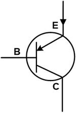 | 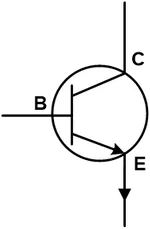 |
Frequently Asked Questions
What parameters does the BJT Cascode Amplifier Calculator compute?
The calculator computes bias voltages (VB1/VB2/VE1/VC1/VC2), currents (IB/IC), transconductance (gm), input resistance (rπ), voltage gain (A), and frequency responses (f1/f2/BW). It uses resistor values, Beta, VBE, and capacitance inputs to determine these parameters via predefined equations .
How is the voltage gain (A) calculated when RE2 is non-zero?
If RE2 (gain control resistor) is not zero, the voltage gain is calculated as A = -(RL || RC) / RE2. This simplifies gain control by directly relating it to the ratio of load/collector resistance and RE2 .
Why is a buffer stage recommended for frequencies above 2MHz?
At frequencies >2MHz, parasitic capacitance (e.g., from scope probes) can degrade bandwidth. A buffer stage (like an emitter follower) isolates the output, preventing loading effects and maintaining frequency response accuracy during measurements .
How does the calculator account for transistor parameters like Beta and VBE?
Beta (DC current gain) and VBE (base-emitter voltage drop) are user-input values. Beta influences base current (IB = (VB1 - VBE)/(RB1 + Beta*RE)), while VBE adjusts emitter voltages (VE1 = VB1 - VBE / VE2 = VB2 - VBE) .
What design choices maximize the amplifier’s bandwidth?
Bandwidth (BW ≈ f1) is maximized by increasing the sum of RE1 and RE2. This reduces the lower pole frequency (f1 = 1/(Rin*(Cbe + 2*Ccb))/(2π)), extending the usable frequency range
Hot SKU
Related Tools
Resistor Color Code Calculator
AIChipLink’s Resistor Color Code Calculator is an interactive tool for identifying resistor values based on 4-band, 5-band, and 6-band color codes. Simply select the colors, and the calculator will display the resistance in Ohms (Ω), tolerance, and power rating. Whether you are building a circuit, repairing electronics, or sorting resistors in your lab, this calculator provides an accurate and efficient way to decode resistor values.
Ohms Law Calculator
AIChipLink’s Ohm’s Law Calculator helps engineers and students quickly calculate resistance, current, voltage, and power in an electrical circuit. Simply enter any two known values, and the calculator will instantly compute the remaining parameters. This fast and easy-to-use online tool illustrates the fundamental relationship between voltage, current, and resistance, making it essential for circuit design, troubleshooting, and electronics learning.
Op-Amp Voltage and Gain Calculator
The Op Amp Voltage and Gain Calculator is an easy-to-use tool for analyzing operational amplifier circuits. It calculates the output voltage, inverting gain, and non-inverting gain based on the input parameters. Simply enter the values of V1, V2, Vp, Vn, and the resistor values R1, R2, R3, and R4, and the calculator will instantly provide accurate results. This tool is suitable for both professional engineers and beginners learning op amp circuit design.
Inverting Op-Amp Resistor Calculator
The Inverting Op Amp Resistor Calculator is a practical tool for analyzing operational amplifier inverting circuits. By entering parameters such as the desired gain, output voltage (Vout), R1 resistance, and the input voltages V1, V2, Vp, and Vn, the calculator automatically determines the required resistor values (R2, R3, and R4). Simply input the values and click “Calculate” to quickly design and verify inverting op amp configurations.
AIChipLink – Your Trusted Electronic Components Distributor
12.28 M
Listed Part Number3,000+
Leading Manufacturers4.9 M
In-stock SKU15,000+
Warehouse Area(㎡)


