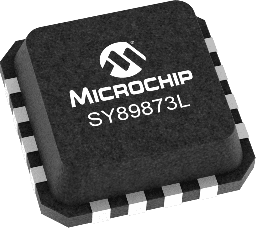

Microchip SY89873LMG
Manufacturer No:
SY89873LMG
Manufacturer:
Microchip
Package:
16-VFQFN Exposed Pad, 16-MLF®
Description:
3.3V LVDS Output Clock Divider/Fanout
Quantity:

In Stock :3777
Looking for price or availability? Send us an RFQ and our sales team will respond quickly.
Shipping & Availability


Fast worldwide shipping via DHL, FedEx, UPS, and EMS.
Shipped from:HK Warehouse
Expected Shipping:Sun, May 31 - Mon, Jun 1, 2026
Lead Time:Inquire about availability
Date Code:Within 2 Years
Payment


We support multiple secure payment methods including PayPal, Visa, MasterCard, and American Express. All transactions are protected with advanced encryption to ensure secure and reliable payments.
Authenticity Guarantee
All components supplied by Aichiplink are sourced from trusted global suppliers and verified through strict in-house inspection and quality control procedures.
Quality Assurance
Certified in-house inspection and testing facilities ensure all components meet internationally recognized quality standards.
User Guide
Aichiplink operates certified in-house inspection and testing facilities to ensure all electronic components meet internationally recognized quality and compliance standards. Our quality management system is verified through ISO 9001 certification and industry-standard inspection procedures.
PURCHASE
Please verify all part numbers, quantities, and packaging preferences before placing your order. If substitutions are acceptable, please indicate this clearly. For time-sensitive projects, confirm estimated delivery dates and stock availability in advance. Once submitted, changes or cancellations may not be possible, especially for items marked as non-cancellable/non-returnable (NCNR). For international shipments, please ensure all import documentation is complete and accurate to avoid delays.
MEANS OF PAYMENTFor your convenience, we accept multiple payment methods in USD, including PayPal, Credit Card, and Wire Transfer. Net terms may be available for qualified customers upon approval.
RFQ (REQUEST FOR QUOTATIONS)Please ensure the part numbers and quantities are accurate and complete when submitting your RFQ.
Provide target prices and acceptable alternatives, if any, to speed up the quotation process.
Quotations are subject to stock availability and may vary with market conditions. Prices and lead times are not guaranteed until a purchase order is confirmed. Ensure your contact details are correct to avoid delays in response.

Step1:Prepare product

Step2:Desiccant Protection

Step3:Vacuum Packaging

Step4:Individual Package

Step5:Anti-collision Filling

Step6:Packaging Box
SHIPPING COST
1. Shipping starts at $40, but some countries will exceed $40. For example (South Africa, Brazil, India, Pakistan, Israel, etc.).
2. Some specific products need to reach the minimum order quantity.
3. It may cost additional remote fees for delivery if you are in a remote area.
Currently, our products are shipped through DHL, FedEx, SF, and UPS.
DELIVERY TIME1. Once the goods are shipped, estimated delivery time depends on the shipping methods you chose: FedEx International, 5-7 business days.
2. For in-stock parts, orders normally could be shipped out within 1-2days.
SY89873LMG Information
Microchip SY89873LMG technical specifications, attributes, parameters and parts with similar specifications to Microchip SY89873LMG.
- Type
- Parameter
- Description
- 2 Banks (÷1, ÷2, ÷4, ÷8, ÷16); 2 Outputs
- Input
- ANY
- Output
- LVDS
- Supply Voltage
- 3.3V
- Max Freq (GHz)
- 2
- Icc (mA)
- 85
- Max Within Device Skew (ps)
- 15
- OE
- True
- Input Mux
- False
- Number Of Outputs
- 0
- Type
- Parameter
- Max Prop Delay (ps)
- 800
Download datasheets and manufacturer documentation for Microchip SY89873LMG.
Data Sheets:

User Guide:
This 3.3V low-skew, low-jitter, precision LVDS output clock divider accepts any high-speed differential clock input (AC- or DC-coupled) CML, LVPECL, HSTL or LVDS and divides down the frequency using a programmable divider ratio to create a frequency-locked, lower speed version of the input clock. The SY89873L includes two output banks. Bank A is an exact copy of the input clock (pass through) with matched propagation delay to Bank B, the divided output bank. Available divider ratios are 2, 4, 8 and 16. In a typical 622MHz clock system this would provide availability of 311MHz, 155MHz, 77MHz or 38MHz auxiliary clock components.
The differential input buffer has a unique internal termination design that allows access to the termination network through a VT pin. This feature allows the device to easily interface to all AC- or DC-coupled differential logic standards. A VREF-AC reference is included for AC-coupled applications.The SY89873L is part of Micrel's high-speed Precision Edge® timing and distribution family. For 2.5V applications, consider the SY89872U. For applications that require an LVPECL output, consider the SY89871U.The /RESET input asynchronously resets the divider outputs (Bank B). In the pass-through function (Bank A) the /RESET synchronously enables or disables the outputs on the next falling edge of IN (rising edge of /N). Refer to the Timing Diagram.
- >2.0GHz fMAX output toggle
- >3.0GHz fMAX input
- <800ps tPD (matched-delay between banks)
- <15ps within-device skew
- <190ps rise/fall time
- <1psRMS cycle-to-cycle jitter
- Unique input termination and VTpin for DC-coupled and AC-coupled inputs: any differential inputs (LVPECL, LVDS, CML, HSTL)
- Precision differential LVDS outputs
- Matched delay: all outputs have matched delay, independent of divider setting
- TTL/CMOS inputs for select and reset/disable
- Bank A: Buffered copy of input clock (undivided)
- Bank B: Divided output (÷2, ÷4, ÷8, ÷16), two copies
- 3.3V power supply
- Wide operating temperature range: -40°C to +85°C
- Available in 16-pin (3mm x 3mm) QFN package
AIChipLink – Your Trusted Electronic Components Distributor
12.28 M
Listed Part Number3,000+
Leading Manufacturers4.9 M
In-stock SKU15,000+
Warehouse Area(㎡)


