

ADI LTC6241CDD#PBF
Manufacturer No:
LTC6241CDD#PBF
Manufacturer:
Package:
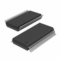
8-WFDFN Exposed Pad
Description:
30mA per Channel 0.2pA 80 dB Instrumentational OP Amps 0.000075μA 2.8V~6V LTC6241 8 Pins 8-WFDFN Exposed Pad
Quantity:
User Guide
Aichiplink operates certified in-house inspection and testing facilities to ensure all electronic components meet internationally recognized quality and compliance standards. Our quality management system is verified through ISO 9001 certification and industry-standard inspection procedures.
Please verify all part numbers, quantities, and packaging preferences before placing your order. If substitutions are acceptable, please indicate this clearly. For time-sensitive projects, confirm estimated delivery dates and stock availability in advance. Once submitted, changes or cancellations may not be possible, especially for items marked as non-cancellable/non-returnable (NCNR). For international shipments, please ensure all import documentation is complete and accurate to avoid delays.
MEANS OF PAYMENTFor your convenience, we accept multiple payment methods in USD, including PayPal, Credit Card, and Wire Transfer. Net terms may be available for qualified customers upon approval.
RFQ (REQUEST FOR QUOTATIONS)Please ensure the part numbers and quantities are accurate and complete when submitting your RFQ.
Provide target prices and acceptable alternatives, if any, to speed up the quotation process.
Quotations are subject to stock availability and may vary with market conditions. Prices and lead times are not guaranteed until a purchase order is confirmed. Ensure your contact details are correct to avoid delays in response.

Step1:Prepare product

Step2:Desiccant Protection

Step3:Vacuum Packaging

Step4:Individual Package

Step5:Anti-collision Filling

Step6:Packaging Box
1. Shipping starts at $40, but some countries will exceed $40. For example (South Africa, Brazil, India, Pakistan, Israel, etc.).
2. Some specific products need to reach the minimum order quantity.
3. It may cost additional remote fees for delivery if you are in a remote area.
Currently, our products are shipped through DHL, FedEx, SF, and UPS.
DELIVERY TIME1. Once the goods are shipped, estimated delivery time depends on the shipping methods you chose: FedEx International, 5-7 business days.
2. For in-stock parts, orders normally could be shipped out within 1-2days.
LTC6241CDD#PBF Information
ADI LTC6241CDD#PBF technical specifications, attributes, parameters and parts with similar specifications to ADI LTC6241CDD#PBF.
- Type
- Parameter
- Lifecycle Status
- PRODUCTION (Last Updated: 3 weeks ago)
- Factory Lead Time
- 8 Weeks
- Mount
- Surface Mount
- Mounting Type
- Surface Mount
- Package / Case
- 8-WFDFN Exposed Pad
- Number of Pins
- 8
- Operating Temperature
- 0°C~70°C
- Packaging
- Tube
- Published
- 2005
- JESD-609 Code
- e3
- Type
- Parameter
- Part Status
- Active
- Moisture Sensitivity Level (MSL)
- 1 (Unlimited)
- Number of Terminations
- 8
- ECCN Code
- EAR99
- Terminal Finish
- Matte Tin (Sn)
- Subcategory
- Operational Amplifier
- Technology
- CMOS
- Terminal Position
- DUAL
- Terminal Form
- NO LEAD
- Peak Reflow Temperature (Cel)
- 260
Download datasheets and manufacturer documentation for ADI LTC6241CDD#PBF.
Datasheets:

ConflictMineralStatement:
LTC6241CDD#PBF Overview
Packaged in a 8-WFDFN Exposed Pad case, the buffer op amp is ready to use. An op amp ic of the General Purpose type. The op amp is delivered to you in a Tube case. There is a growing number of terminations approaching the number of 8. The pins on this board total to 8 in total. I would like to remind you that this buffer op amp should be powered by an 3V battery. I would like to specify that this buffer amplifier belongs to the Operational Amplifier-type of devices. A total of 8 pins are present on the instrumentation amplifier. There is an input offset voltage of 100μV for this buffer op amp. The mounting type that is recommended for this electrical part is Surface Mount. In relation to the operating temperature of this buffer op amp, it works well at an average of 0°C~70°C . As long as the supply current of the chip does not exceed 1.8mA, this op amp ic can operate. 124.08dB should remain the voltage gain. During the manufacturing process, this buffer amplifier is divided into 2 circuits. One of the many advantages that this linear amplifier has, among many other things, is the fact that it outputs Rail-to-Rail signals. The linear amplifier consists of 2 different elements in total.
LTC6241CDD#PBF Features
8 Pins
supply voltage of 3V
124.08dB voltage gain
Output Type: Rail-to-Rail
LTC6241CDD#PBF Applications
There are a lot of Linear Technology/Analog Devices
LTC6241CDD#PBF Instrumentational OP Amps applications.
- Integrator circuits
- Differentiator circuits
- Logarithmic operation circuits
- Exponential operation circuits
- Multiplication circuits
- Division circuits
- Precision measurement
- Power control
- Information processing
- Weak signal detection
LTC6241CDD#PBF Relevant information


The following parts are popular search parts in Integrated Circuits (ICs).
In Stock :Available
Looking for price or availability? Send us an RFQ and our sales team will respond quickly.
Shipping & Availability


Fast worldwide shipping via DHL, FedEx, UPS, and EMS.
Payment


We support multiple secure payment methods including PayPal, Visa, MasterCard, and American Express. All transactions are protected with advanced encryption to ensure secure and reliable payments.
Authenticity Guarantee
All components supplied by Aichiplink are sourced from trusted global suppliers and verified through strict in-house inspection and quality control procedures.
Quality Assurance
Certified in-house inspection and testing facilities ensure all components meet internationally recognized quality standards.
AIChipLink – Your Trusted Electronic Components Distributor
12.28 M
Listed Part Number3,000+
Leading Manufacturers4.9 M
In-stock SKU15,000+
Warehouse Area(㎡)