How to Read Amplifier Circuit Symbols and Op-Amp Schematics
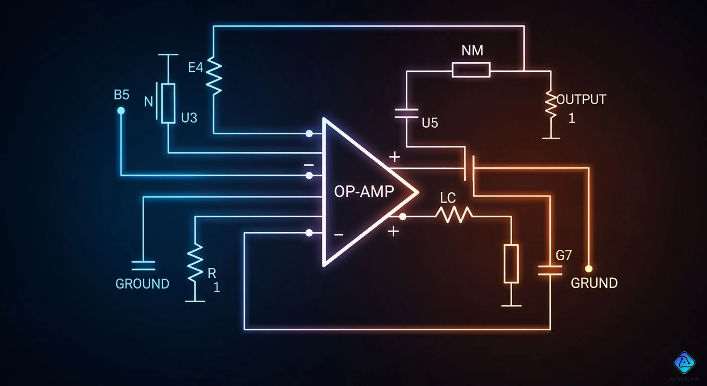
When reading amplifier circuit symbols, you will see a triangle shape. This main op-amp symbol stands for the basic operational amplifier part. The left side has a non-inverting input with a plus sign. Next to it, an inverting input has a minus sign. Every non-inverting input pairs up with an inverting input line. Both lines get a voltage signal from sources on the left. The pointed end forms an output terminal that carries output voltage. You can trace this output signal along a path to loads on the right, where feedback changes an inverting symbol. Do not mix up a schematic symbol with a chip diagram. Real hardware uses physical pins, but an op-amp symbol makes an inverting layout easier to read as a single op-amp symbol.
Key Takeaways
-
In electronic drawings, a triangle shape stands for an operational amplifier circuit.
-
Plus and minus signs show the input connection points on the symbol.
-
Resistors linked from the output to the input control the signal increase.
-
Datasheet pin numbers connect the diagram symbols to real hardware chips.
Understanding Op Amp Symbol Anatomy
Input and Output Terminals in Circuit Diagrams
When reading amplifier circuit symbols, you will notice a simple triangle shape. An operational amplifier drawing uses a clear op amp symbol to show the part. Your source signal goes into the non-inverting input marked with a plus sign. Meanwhile, the inverting input marked with a minus sign forms an inverting setup.
| Symbol Marking | Terminal Identification |
|---|---|
| + | non-inverting input |
| − | inverting input |
Every non-inverting input terminal pairs up directly with an inverting input terminal. An input voltage enters through a non-inverting input pin, while an inverting input connection allows inverting feedback. High input impedance keeps an input path from pulling much current. A classic 741 bipolar chip gives you 2 Megohms of input impedance. Newer FET devices can reach 1 TΩ of input impedance. The pointed tip acts as the output side. In a closed loop, an open-loop TL081 output resistance drops below 1Ω at DC. With a signal frequency of 100 Hz, output impedance equals 4.5 mΩ. The value becomes 1 Ω at 10 kHz and reaches 45 Ω at 1 MHz. This low output impedance easily sends an output signal to power an output load cleanly.
Power Supply Rails on Operational Amplifier Symbols
Any op amp symbol needs power to run the rest of your circuit. Official IEEE/ANSI guidelines place power rails directly on an operational amplifier drawing. These power pins link to your positive and negative voltage rails. Without this main DC voltage supply, the part cannot produce any output action.
Engineers frequently tweak an op amp symbol to save extra room. Modern software programs like KiCad divide dual packages into individual units. As an example, unit U1A acts as an active amplifier section. At the same time, unit U1C carries the power pins for V+ and V-. This split schematic symbol layout creates a much cleaner schematic symbol view. Another simplified op amp symbol might hide these supply lines entirely. Using a clean op amp symbol helps you trace every signal path in your circuit easily. An op amp symbol helps you spot each inverting input, non-inverting input, output line, output pin, and voltage rail fast.
Tracing Feedback in Operational Amplifier Circuits
Negative Feedback in Amplifier Topologies
Tracing feedback loops on a diagram shows you how a circuit works. An operational amplifier puts extra parts between its output and input terminals. An op amp symbol uses a feedback line that loops back to an inverting input. This closed loop drops the total gain and keeps the circuit stable.
In an inverting amplifier design, a feedback resistor links the output terminal to an inverting input pin. Another resistor connects your source signal to that same point. This pair of resistors sets how the circuit acts. The closed-loop gain uses a simple math formula to find your output voltage.
| Configuration | Closed-Loop Gain Formula |
|---|---|
| Inverting | -Rf/Rin |
| Non-inverting | 1 + Rf/Rin |
Your source signal goes straight into a non-inverting input terminal. Using negative feedback raises input impedance for non-inverting circuits. Meanwhile, an inverting amplifier sets its input impedance to match its input resistor value.
A simple voltage follower links its output directly to an inverting input. This special setup gives your circuit a total gain of one. Engineers use a voltage follower to protect weak signal sources from heavy output loads.
Open-Loop Configurations and Comparators
An operational amplifier works in open-loop mode when you leave off the feedback loop. High open-loop gain pushes your output voltage to the power rails quickly. A small voltage difference between inputs sends the part into full saturation. You can use this fast open-loop action to build a working comparator circuit.
A basic comparator checks the voltage level between two separate input lines. You will see a comparator used in threshold detector setups. The main signal enters through the non-inverting input line. A steady reference signal links to the inverting input pin. The op amp symbol shows no feedback parts returning to an inverting input.
| Configuration | Input Connection | Output Equation | Key Behavior |
|---|---|---|---|
| Differential | Both inputs have signals | Vout = A(Vi1 - Vi2) | Amplifies difference between two signals |
| Inverting | Signal on inverting pin, non-inverting pin grounded | Vout = -AVi | Output is 180° out of phase |
| Non-Inverting | Signal on non-inverting pin, inverting pin grounded | Vout = AVi | Output easily hits saturation rail |
A comparator symbol uses the same triangle shape as a regular amplifier symbol. However, this comparator part acts like a digital switch to make quick logic decisions.
The open-loop gain of an operational amplifier is the gain obtained when no overall feedback is used. An ideal op-amp has infinite open-loop gain, while a typical op-amp may have a maximal open-loop gain of around 10^5 (100 dB).
Your output voltage jumps high whenever a non-inverting input drops higher than an inverting input.
-
Positive saturation state:
VOUT = +Vcc. -
Negative saturation state:
VOUT = –Vcc.
Unwanted input noise causes quick output switching near your trigger point. You can add positive feedback to a comparator to create hysteresis. Hysteresis stops output chatter caused by signal noise in your comparator circuit. A comparator with hysteresis sets upper and lower switching levels. Every comparator relies on its power supply rails to define output limits. You can spot a comparator by finding an open-loop layout on your schematic. A drawn symbol shows the exact signal path through your circuit components. An op amp symbol without feedback signals a comparator design. This clear op amp symbol makes reading schematics simple. Every symbol helps you learn good diagram reading skills.
Mapping Amplifier Circuit Symbols to Hardware
Connecting Schematic Terminals to IC Pins
You match amplifier circuit symbols to real hardware parts when building a project. A schematic symbol puts signal lines where they look best on paper. Real integrated circuit chips put physical pins around a plastic case instead. You find Pin 1 by looking for a small dot, notch, or corner line on the chip. Then, count the pins counterclockwise looking down from above.
Datasheets map every op amp symbol terminal to real hardware pins.
| IC | Package | Non-Inverting Input Pin(s) | Inverting Input Pin(s) | Output Pin(s) |
|---|---|---|---|---|
| LM741 (Single) | 8-pin | Pin 3 | Pin 2 | Pin 6 |
| LM358 (Dual) | 8-pin | Pins 3, 5 | Pins 2, 6 | Pins 1, 7 |
| LM324 (Quad) | 14-pin | Pins 3, 5, 10, 12 | Pins 2, 6, 9, 13 | Pins 1, 7, 8, 14 |
An open op amp symbol splits up power lines to make diagrams easier to follow. This clean schematic symbol plan helps guide your wiring work on a breadboard. Each op amp symbol maps every single terminal directly to real IC pins.
Handling 741 IC Pinouts and Dual Packages
The classic 741 chip shows how hardware pins connect to a diagram. You wire parts to these specific pins:
-
Pin 1 and Pin 5: Offset Null pins for manual adjustments
-
Pin 2: Inverting input pin for feedback wires
-
Pin 3: Non-inverting input pin for direct signals
-
Pin 4 and Pin 7: Negative and positive power supply pins
-
Pin 6: Main output lead for sending amplified voltage
-
Pin 8: N/C pin with no internal circuit connection
This terminal layout delivers your signal out of Pin 6 to drive your output loads. That symbol drawing helps you spot chip pins fast.
Dual-op-amp packages place two full operational amplifier units inside one chip. Unit A uses Pin 2 as its primary inverting input line. Unit B uses Pin 6 as its own inverting input connection. Extra amplifier units inside dual packages need proper wiring to keep your circuit stable. You can connect an extra inverting input straight to its output pin. Wiring the extra non-inverting input terminal to ground stops random noise from entering active paths. Wiring extra package pins correctly keeps all your active signal lines safe. This setup makes sure every output channel runs smoothly.
Reading amplifier circuit symbols requires a clear workflow. First, locate non-inverting input and inverting input on your operational amplifier triangle symbol. Next, trace the feedback path from the output terminal back to an inverting input connection. Match every op amp symbol to chip symbol pins.
Follow this pre-power checklist before testing your circuit:
-
Confirm positive supply voltage and negative voltage polarity on power pins.
-
Check continuity between an output lead and an inverting lead on package pins.
-
Verify notch orientation so physical pins align with your schematic symbol layout.
-
Ground any unused inverting input to prevent signal noise on IC pins near an op amp symbol board symbol.

Written by Jack Elliott from AIChipLink.
AIChipLink, one of the fastest-growing global independent electronic components distributors in the world, offers millions of products from thousands of manufacturers, and many of our in-stock parts is available to ship same day.
We mainly source and distribute integrated circuit (IC) products of brands such as Broadcom, Microchip, Texas Instruments, Infineon, NXP, Analog Devices, Qualcomm, Intel, etc., which are widely used in communication & network, telecom, industrial control, new energy and automotive electronics.
Empowered by AI, Linked to the Future. Get started on AIChipLink and submit your RFQ online today!
Frequently Asked Questions
What does the triangle symbol represent in schematics?
The triangle symbol represents an operational amplifier or a comparator unit. This shape directs the flow of signals from left inputs to the right output. It clearly shows the difference between the inverting terminal and the non-inverting line.
How do you identify inverting pins on physical chips?
You can locate inverting pins by checking the chip datasheets. Pin 2 acts as the main terminal on a standard LM741 chip. Dual packages feature extra pins for different channels. You simply match each schematic symbol to the physical hardware pins.
Why do open loop amplifiers lack feedback?
Open loop designs work without any feedback path in place. This setup compares the voltage levels between both input terminals. A comparator symbol shows no parts returning to the negative input. The circuit pushes the output to maximum saturation voltage very fast.
What is the main purpose of a voltage follower?
A voltage follower links the output line straight back to the inverting pin. You spot this symbol by tracing a line from the output to the input. Grounding extra unused pins stops unwanted noise while maintaining high input impedance. You can safely ground these extra pins.