

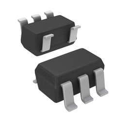
Renesas 83115BRLFT
Manufacturer No:
83115BRLFT
Manufacturer:
Package:
QSOP
Description:
1 Circuit 200MHz 3.3V Clock Buffer DUAL 28 Pins QSOP
Quantity:

In Stock :Available
Looking for price or availability? Send us an RFQ and our sales team will respond quickly.
Shipping & Availability


Fast worldwide shipping via DHL, FedEx, UPS, and EMS.
Payment


We support multiple secure payment methods including PayPal, Visa, MasterCard, and American Express. All transactions are protected with advanced encryption to ensure secure and reliable payments.
Authenticity Guarantee
All components supplied by Aichiplink are sourced from trusted global suppliers and verified through strict in-house inspection and quality control procedures.
Quality Assurance
Certified in-house inspection and testing facilities ensure all components meet internationally recognized quality standards.
User Guide
Aichiplink operates certified in-house inspection and testing facilities to ensure all electronic components meet internationally recognized quality and compliance standards. Our quality management system is verified through ISO 9001 certification and industry-standard inspection procedures.
Please verify all part numbers, quantities, and packaging preferences before placing your order. If substitutions are acceptable, please indicate this clearly. For time-sensitive projects, confirm estimated delivery dates and stock availability in advance. Once submitted, changes or cancellations may not be possible, especially for items marked as non-cancellable/non-returnable (NCNR). For international shipments, please ensure all import documentation is complete and accurate to avoid delays.
MEANS OF PAYMENTFor your convenience, we accept multiple payment methods in USD, including PayPal, Credit Card, and Wire Transfer. Net terms may be available for qualified customers upon approval.
RFQ (REQUEST FOR QUOTATIONS)Please ensure the part numbers and quantities are accurate and complete when submitting your RFQ.
Provide target prices and acceptable alternatives, if any, to speed up the quotation process.
Quotations are subject to stock availability and may vary with market conditions. Prices and lead times are not guaranteed until a purchase order is confirmed. Ensure your contact details are correct to avoid delays in response.

Step1:Prepare product

Step2:Desiccant Protection

Step3:Vacuum Packaging

Step4:Individual Package

Step5:Anti-collision Filling

Step6:Packaging Box
1. Shipping starts at $40, but some countries will exceed $40. For example (South Africa, Brazil, India, Pakistan, Israel, etc.).
2. Some specific products need to reach the minimum order quantity.
3. It may cost additional remote fees for delivery if you are in a remote area.
Currently, our products are shipped through DHL, FedEx, SF, and UPS.
DELIVERY TIME1. Once the goods are shipped, estimated delivery time depends on the shipping methods you chose: FedEx International, 5-7 business days.
2. For in-stock parts, orders normally could be shipped out within 1-2days.
83115BRLFT Information
Renesas 83115BRLFT technical specifications, attributes, parameters and parts with similar specifications to Renesas 83115BRLFT.
- Type
- Parameter
- Factory Lead Time
- 10 Weeks
- Contact Plating
- Tin
- Mount
- Surface Mount
- Package / Case
- QSOP
- Number of Pins
- 28
- Published
- 2003
- JESD-609 Code
- e3
- Pbfree Code
- yes
- Part Status
- Active
- Moisture Sensitivity Level (MSL)
- 1 (Unlimited)
- Type
- Parameter
- Number of Terminations
- 28
- ECCN Code
- EAR99
- Max Operating Temperature
- 70°C
- Min Operating Temperature
- 0°C
- Subcategory
- Clock Drivers
- Terminal Position
- DUAL
- Terminal Form
- GULL WING
- Peak Reflow Temperature (Cel)
- 260
- Number of Functions
- 1
- Supply Voltage
- 3.3V
Download datasheets and manufacturer documentation for Renesas 83115BRLFT.

83115BRLFT Overview
There is a case available for the cut smart buffer in QSOP. For normal operation, 200MHz is the maximum value. It has 28 terminations in it, which means that it is terminated. Supply voltages of 3.3V are capable of achieving high efficiency. It has been positioned in the way of Surface Mount. There are 28 pins on the clock buffer. During operation, 28 pins are used. I have enclosed this circuit clock in Clock Drivers for your convenience. The clock switch operates at a minimum working temperature of 0°C in order to maintain reliability. It is possible to achieve stable operation by setting the maximum operating temperature to 70°C. The circuit uses a logic IC with a value of LOW SKEW CLOCK DRIVER as the input. As a default, it is set to output 16. A maximum supply voltage of 3.465VV can be applied to it. Depending on the type of source voltage, it can run with a voltage as low as 3.135V. When the supply voltage is at 3.3V, the efficiency will be highest.
83115BRLFT Features
28 terminations
Clock Drivers subcategory
logic IC type of LOW SKEW CLOCK DRIVER
83115BRLFT Applications
There are a lot of Integrated Device Technology (IDT)
83115BRLFT Clock Buffers & Drivers applications.
- Clock signal format conversion
- Clock signal level shifting
- High performance communication system
- Data center
- Cloud computing
- Network
- High speed industry
- High-end consumer electronics
- Data communication
- Telecommunications
83115BRLFT Relevant information


.png&w=256&q=75)


The following parts are popular search parts in Integrated Circuits (ICs).
AIChipLink – Your Trusted Electronic Components Distributor
12.28 M
Listed Part Number3,000+
Leading Manufacturers4.9 M
In-stock SKU15,000+
Warehouse Area(㎡)