
Introduction
In the rapidly evolving semiconductor industry, technological roadmaps serve as essential tools for forecasting trends, guiding research and development, and setting industry standards. One such influential roadmap is the International Technology Roadmap for Semiconductors (ITRS), which has undergone multiple iterations over the years. The ITR2010 was a significant milestone in the roadmap series, addressing crucial aspects of semiconductor scaling, emerging materials, and advanced manufacturing techniques.
This blog will provide an in-depth analysis of ITR2010, comparing it with previous versions, discussing its impact on the semiconductor industry, and answering frequently asked questions (FAQs) related to the roadmap.
What is ITR2010?
The ITR2010, also known as BY-ITR2010, is a component referred to as a "Slot Optical Switch." It consists of two main parts:
• Gallium Arsenide Infrared Emitting Diode (LED): This component emits infrared light. Gallium arsenide is a semiconductor material commonly used for infrared LEDs because it emits light in the infrared spectrum, which is not visible to the human eye.
• Silicon Phototransistor: The emitted infrared light is detected by a silicon phototransistor. Phototransistors are semiconductor devices that can be used to detect light and convert it into an electrical signal.
These components are housed together in a plastic housing. The design of the housing is optimized for several key characteristics:
• Mechanical Resolution: It is designed to ensure precise alignment between the LED and phototransistor, allowing for accurate light detection.
•Coupling Efficiency: The housing is designed to maximize the efficiency of the light transmission between the LED and phototransistor, ensuring reliable operation.
• Ambient Light Isolation: The housing is also designed to block out ambient light, which can interfere with the proper functioning of the device. This is important in applications where the device needs to reliably detect changes in light, such as when an opaque material interrupts the light path.
The "slot" in the housing allows for the interruption of the light signal. When an opaque material, such as paper in a printer, passes through the slot, it blocks the infrared light, causing the output of the phototransistor to switch from an "ON" state to an "OFF" state. This feature is useful in a variety of applications, including printers, scanners, copiers, and any other devices that require the detection of physical objects or interruptions in a light path.
The International Technology Roadmap for Semiconductors (ITRS) 2010 edition (ITR2010) was published to outline the future directions for semiconductor technology. The roadmap analyzed key challenges and solutions for scaling integrated circuits (ICs), incorporating insights from industry leaders, academia, and research institutions.
ITR2010 addressed key topics such as:
• More Moore Scaling – Continued miniaturization of transistors following Moore’s Law.
• More than Moore (MtM) – Heterogeneous integration of functionalities beyond digital scaling.
• Emerging Research Devices (ERD) – Development of novel transistor technologies such as tunnel FETs and spintronics.
• Advanced Manufacturing & Lithography – The introduction of extreme ultraviolet (EUV) lithography.
Absolute Maximum Ratings

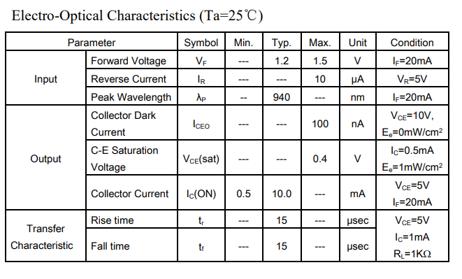
Electro-Optical Characteristics
Package (Unit: mm)
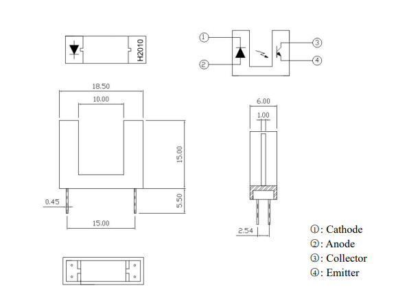
CAD Model

Applications
• Mouse: It can be used in computer mice to detect the movement of the mouse by interrupting the light beam when the mouse is moved.
• Copier: In photocopiers, the ITR2010 can be used for various purposes, such as detecting paper movement or jamming, or for document feeding.
• Switch Scanner: It can be used in switch scanning applications, where it detects the position of switches or buttons, providing input to electronic devices.
• Floppy Disk Driver: While floppy disk drives are less common today, the ITR2010 may have been used in the past to detect the presence of a floppy disk or to monitor its rotation.
• Non-contact Switching: In non-contact switching applications, the ITR2010 can be used to detect the presence or absence of an object without physical contact, making it suitable for various automation and sensing tasks.
• For Direct Board: This could indicate that it's suitable for direct mounting on a circuit board, making it versatile for integration into various electronic devices and systems.
Manufacturer
The ITR2010 photointerrupter is manufactured by Everlight Electronics Co., Ltd. Everlight Electronics Co., Ltd. is a well-known Taiwanese company that specializes in the manufacturing of optoelectronic components. Established in 1983, Everlight has grown to become one of the world's leading manufacturers of LEDs (light-emitting diodes), optocouplers, infrared components, and various other optoelectronic products. The company's product portfolio includes a wide range of components used in various applications, including consumer electronics, automotive lighting, industrial automation, medical devices, and more.
Key Differences: ITR2010 vs. Previous Editions
To better understand the advancements introduced in ITR2010, let’s compare it with its predecessor, ITR2007.
| Feature | ITR2007 | ITR2010 |
|---|---|---|
| Transistor Scaling | Focused on continued CMOS scaling | Addressed scaling limits and alternative device architectures |
| Lithography | 193nm immersion lithography | Introduction of EUV lithography for sub-22nm nodes |
| Power Management | Increased power efficiency concerns | Emphasized power-aware design and low-power technologies |
| 3D Integration | Conceptual discussion | Advanced research on 3D IC stacking |
| More than Moore (MtM) | Limited discussion on heterogeneous integration | Strong emphasis on analog, RF, MEMS, and bioelectronics |
| New Materials | Initial research on high-k dielectrics and metal gates | Focus on new materials like graphene, III-V compounds, and carbon nanotubes |
As the table illustrates, ITR2010 built upon the foundation laid by ITR2007, incorporating advancements in materials, power management, and integration techniques.
Impact of ITR2010 on the Semiconductor Industry
ITR2010 had a significant influence on semiconductor technology and industry trends. Below are some of its key impacts:
1. Scaling Beyond Moore’s Law
While traditional CMOS scaling was reaching physical limits, ITR2010 provided a framework for post-CMOS technologies, exploring new transistor architectures, material innovations, and 3D stacking.
2. Advancements in Lithography
One of the most critical aspects of ITR2010 was the introduction of extreme ultraviolet (EUV) lithography, which later became a crucial technology in manufacturing sub-7nm chips.
3. Energy Efficiency & Power Optimization
Power efficiency emerged as a significant challenge, leading to the development of low-power semiconductor designs, including FinFET transistors that were later widely adopted.
4. More-than-Moore Applications
ITR2010 recognized the importance of functionalities beyond digital scaling, leading to advancements in RF, MEMS, and biomedical semiconductor technologies.
5. Material Innovations
The roadmap accelerated research on new materials like graphene and III-V compounds, paving the way for next-generation semiconductor technologies.
Frequently Asked Questions (FAQs)
Q1: What was the purpose of ITR2010?
ITR2010 aimed to guide the semiconductor industry by forecasting technological challenges and potential solutions for the next 15 years.
Q2: How did ITR2010 differ from previous versions?
Compared to earlier versions like ITR2007, ITR2010 introduced EUV lithography, emphasized More than Moore concepts, and addressed power consumption challenges more comprehensively.
Q3: Did ITR2010 predict the end of Moore’s Law?
ITR2010 acknowledged that traditional CMOS scaling faced severe limitations and encouraged research into alternative transistor architectures and new materials.
Q4: What technologies were influenced by ITR2010?
ITR2010 significantly influenced the adoption of FinFET transistors, EUV lithography, 3D IC stacking, and heterogeneous integration in modern semiconductor design.
Q5: How relevant is ITR2010 today?
Although newer roadmaps have since replaced ITR2010, many of its predictions and focus areas—such as low-power design, new materials, and 3D integration—remain critical in today's semiconductor landscape.
Conclusion
ITR2010 played a crucial role in shaping the semiconductor industry's trajectory by addressing key challenges in transistor scaling, lithography, power management, and material innovation. While the industry has since moved beyond some of its predictions, many of its concepts continue to influence semiconductor advancements today.
For semiconductor professionals, researchers, and engineers, understanding ITR2010 provides valuable insights into the industry's evolution and the foundations of modern chip manufacturing. As we move into the era of AI-driven computing, quantum semiconductors, and advanced 3D integration, the lessons from ITR2010 remain highly relevant.
Written by Icey Ye from AIChipLink.
AIChipLink, one of the fastest-growing global independent electronic component distributors in the world, offers millions of products from thousands of manufacturers. Whether you need assistance finding the right part or electronic components manufacturers for your design, you can contact us via phone, chat or e-mail. Our support team will answer your inquiries within 24 hours.